Page 19 - ChipScale_Jul-Aug_2020-Digital
P. 19
thermal and interference, the packaging
                                                                              is the main tool to handle such issues.
                                                                              The latest advance in this field is
                                                                              produced for Broadcom (formerly
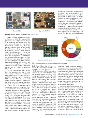
                                                                              Avago). As shown in Figure 3, a new
                                                                              type of double-side BGA packaging
                                                                              technology has emerged from Amkor,
                                                                              which produces a very cost-effective,
                                                                              small form factor and high-performance
                                                                              component offering full compatibility
                                                                              on the mid/high 4G frequency band.
                                                                                Several innovations have led to the
                                                                              kind of high-end packaging discussed
                                                                              above. The first and most well-known
        Figure 2: Murata vs. Skyworks: module opened view. SOURCES: [2,3]
          LGA is the most common packaging
        technology for RF. In this structure, the
        passive or active components are always
        with the lowest interconnection to the
        supporting substrate (printed circuit
        board [PCB], ceramic, etc.). Also, the
        capping (molding, metal lid, etc.) could
        be different depending on the thermal
        budget of the device. On the module
        side, the most advanced LGA serves
        the single band in 4G implementation,
        low-, mid- or high-band. Depending on
        the supplier, different versions of LGA
        technology could apply. If we consider
        the low-band power amplifier module
        integrated duplexer (LB-PAMiD), we
        observe, for example, the two different   Figure 3: Broadcom opening and component cost breakdown. SOURCE: [4]
        SiP architectures using LGA from   [2,3]. We could say that for these two   technology is the conformal shielding
        Murata and Skyworks, as shown in   devices, the main influence on the cost   that isolates the internal structure. The
        Figure 2.                          came from the LTCC substrate.      second is the compartmental shielding.
          The two components noted above     Today, however, LGA packaging    Several assembly players have developed
        have the same purpose. One is built   has become less interesting for high-  a process to realize such functionality.
        on a ceramic substrate – a 10-layer   end suppliers facing the rise of BGA   The most popular method is with a hole
        low-temperature co-fired ceramic   packaging technology. As the industry is   realized by laser drilling and filled with
        (LTCC) – and the other on a 6-layer   looking for a way to integrate 5G along   solder paste. This new development
        PCB substrate. Also, the number of   with high-performance 4G, packaging   allows the evolution of the technique
        dies and the packaging are not exactly   has to evolve in order to provide a   to use wire bonding connected to the
        the same for both. Murata chose to   solution to reduce the form factor while   conformal shielding either at the top, or
        integrate a plurality of filters with   keeping the relatively high-performance   at the sides of the package.
        a coupler and is using conformal   level. A new module — low-noise power   Amkor has also proposed some wire
        shielding to protect the component from   amplifier module integrated duplexer   fences that directly connect the conformal
        electromagnetic interference (EMI).   (L-PAMiD) — has been seen recently   shielding at the top of the package to
        Skyworks, however, is more traditional,   featuring mid-/high-band compatibility,   the PCB substrate at the bottom. The
        yet more innovative in terms of filtering   and even a full-band 4G diversity   third and final technology is the double-
        technology. Only four surface acoustic   module (SKY53735) has come about.   side molding, which is a way to mount a
        wave (SAW) filters are integrated into   For the full-band 4G diversity module,   component die at each side of the PCB
        the Skyworks packaging along with   it’s the technology (silicon on insulator   substrate. On one side the dies are over
        several bare dies connected to the PCB   [SOI] and SAW filter) that enables the   molded, and on the other side the dies are
        substrate with gold wire bonding. Both   innovation. For the mid-/high-band   flip-chipped using thermocompression
        packages have roughly the same area,   L-PAMiD, the packaging is the key   bonding with an underfill. By doing
        whereas Skyworks’s PAMiD has a cost   enabler for such high integration. This   so, the bottom dies are isolated from
        that is 49% lower than Murata’s. As   has come with new challenges, such as   the internal components while the PCB
        usual, we estimate that almost 40%   internal isolation, external isolation, and   substrate required for the devices is
        of the component cost came from the   high-sensitivity component isolation.   drastically reduced [4]. This integration
        packaging, including the substrate cost   In fact, when the major concerns are

                                                                                                             17
                                                             Chip Scale Review   July  •  August  •  2020   [ChipScaleReview.com]  17

