Page 24 - ChipScale_Jul-Aug_2020-Digital
P. 24
Solder stock is supplied in three main
        forms: paste, preform (freeform/pre-
        applied on substrate/die backside), and
        wire. Solder paste is most commonly
        deployed by means of a stencil-printing
        process. The solder paste must be tacky
        enough to secure the components in
        place throughout the production process,
        especially until the reflow process.
          During the ref low process, tight
        control of the temperature profiles is
        extremely important. The temperature
        rate of increase must be slow enough to
        prevent solder balling, while also being
        fast enough not to deplete the flux. The
        ultimate temperature needs to be as
        low as possible to avoid damage, but
        still high enough to fully activate the
        flux, melt the solder itself, and allow
        for adequate wetting. Cooling should
        be quick enough to retain the desired
        shape and prevent oxidation, while slow
        enough to control substrate warpage.
          There are several possibilities to
        dispense solder wire, which can be
        provided flux-less, thereby eliminating
        f lux residue issues. An established
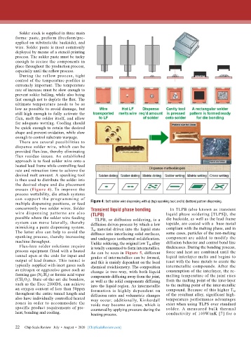
        approach is to feed solder wire onto a
        heated lead frame while controlling feed
        rate and retraction time to achieve the
        desired melt amount. A spanking tool
        is then used to distribute the solder into
        the desired shape and die placement
        ensues (Figure 4). To improve the
        process wettability, die attach systems
        can  suppor t  the prog ram ming  of
        multiple dispensing positions, or feed   Figure 4: Soft solder wire dispensing with a) (top) spanking tool; and b) (bottom) pattern dispensing.
        concurrently two solder wires. Solder   Transient liquid phase bonding   In TLPB (also known as transient
        wire dispensing patterns are also   (TLPB)                            liquid phase soldering [TLPS]), the
        possible where the solder wire feeding   TLPB, or diffusion soldering, is a   die backside, as well as the lead frame
        system can  move  laterally,  thereby   diffusion-driven process by which a low   topside, are coated with a  base metal
        mimicking a paste dispensing system.   T M  material driven into the liquid state   compliant with the melting phase, and in
        The latter also can help to avoid the   diffuses into interfacing solid surfaces,   some cases, particles of the non-melting
        spanking process, thereby increasing   and undergoes isothermal solidification.   component are added to modify the
        machine throughput.                Unlike soldering, the original low T M  alloy   diffusion behavior and control bond line
          Flux-less solder solutions require   is totally consumed to form intermetallics.   thicknesses. During the bonding process,
        process equipment fitted with a heated   As can be seen in Figure 5, different   force and heat are combined until the
        tunnel open at the ends for input and   grades of intermetallics can be formed,   liquid interlayer melts and begins to
        output of lead frames. This tunnel is   and this is mainly dependent on the local   react with the base metals to create the
        typically supplied with inert gases such   chemical stoichiometry. The composition   intermetallic compounds. After the
        as nitrogen or aggressive gases such as   change is two-way, with both liquid   consumption of the interlayer, the re-
        forming gas (N 2 :H 2 ) or formic acid vapor   components diffusing away from the joint,   melting temperature of the joint rises
        (CH 2 O 2 ). State-of-the-art die bonders,   as well as the solid components diffusing   from the melting point of the inter-layer
        such as the Esec 2100DS, can achieve   into the liquid region. As intermetallic   to the melting point of the inter-metallic
        an oxygen content of less than 50ppm   formation  is highly  dependent  on   compound. Because of this higher T M
        throughout the entire tunnel length and   diffusion rates and volumetric changes   of the resultant alloy, significant high-
        also have individually controlled heated   may occur; additionally, Kinkerdall   temperature performance advantages
        zones in order to accommodate the   voids may become an issue, which is   exist when using TLPS over standard
        specific product requirements of pre-  countered by applying pressure during the    solder. A measured bulk ther mal
        heat, bonding and cooling.         heating process.                   conductivity  of  140W/mK  [7]  for  a


        22   Chip Scale Review   July  •  August  •  2020   [ChipScaleReview.com]
        22

