Page 26 - ChipScale_Jul-Aug_2020-Digital
P. 26
Cu /Sn /Cu system has                                                           60 minutes held at 200°C.
        been reported, however                                                          The resultant bond material
        weak interfaces formed                                                          thermal conductivity would
        across intermetallics,                                                          ultimately be in the range
        together  with  reduced                                                         of 70-150W/mK, depending
        elast icit y because of                                                         on the particle chemistry
        the intermetallic´s high                                                        and particle size distribution
        mo d u l u s ,  c a n  l i m i t                                                (PSD) loading, together with
        application of TLPS in                                                          the epoxy formulation.
        very high-power density                                                           Semi-sintering media
        applications.                                                                   have found good use in mid-
                                                                                        to high-power applications
        Hybrid pastes/semi-                                                             w h e r e t h e s i g n i f i c a n t
        sintering pastes                                                                processing time is countered
          Compared to soldering                                                         b y  t h e  e l i m i n a t i o n  of
        and TLPS, the sintering                                                         intermetallics, good thermal
        process does not require                                                        c o n d u c t iv it y,  t u n a b l e
        a phase change of the                                                           mo du lu s r a ng i ng f rom
        metal components and no                                                         approximately 2–20GPa,
        melting occurs. Sintering                                                       and the relative simplicity of
        can be achieved either                                                          curing without the need of a
        without using any pressure                                                      sinter press.
        when using hybrid semi-
        sintering pastes, or by                                                         Pressure sintering
        using pressure for a fully                                                        Time, temperature and
        metallic bond.                                                                  pressure are key enablers for
          Hybrid semi-sintering                                                         neck formation and fusion of
        pastes are broadly similar                                                      particles in pressure-assisted
        to ICAs as the sinter                                                           sintering. The externally
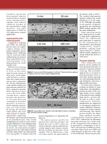
        material stock consists of   Figure 5: Cross-sectional SEM micrographs of Cu/Sn/Cu TLP bonded interfaces subjected   applied force is required to
                               to bonding at 300°C for various durations adapted from [6].
        three parts: silver/copper                                                      push the particles closer to
        solid particles in micro-                                                       each other, thereby squeezing
        flake form, liquid solvents,                                                    out voids, promoting cohesion,
        and an epoxy component                                                          and ultimately achieving a
        [8]. The key differentiator                                                     fully-metallic sinter layer.
        is the metallic loading and                                                       For nano-sinter particles,
        final structure achieved. In                                                    necking can initiate at room
        ICAs, conductive particles                                                      temperature and atmospheric
        allow electrons to move                                                         pressure because of the very
        across the bulk either                                                          large surface area to volume
        through direct contact                                                          of the particles and resultant
        between the particles,                                                          high surface activity [4].
        o r t h r ou g h q u a n t u m                                                  In order to achieve room-
        tunneling  of  proximal                                                         t e mp e r a t u r e  st a bi l it y,
        m e t a l li c  i n t er f ac e s .                                             nanoparticles are engineered
        Hybrid sintering, however,                                                      to incorporate proprietary
        goes one step fur ther                                                          surface stabilizers, which are
        by having the metallic                                                          designed to protect against
        fillers diffuse into each   Figure 6: Cross section of semi-sintered micron-sized flake particles in a cured epoxy   self-sintering. The typical
        other (Figure 6), thereby   resin. COURTESY: MacDermid Alpha                    process profile for sinter
        significantly improving            property degradation as T J  approaches the   paste products includes
        the thermal and mechanical properties   epoxy T G .                   a drying profile of printed paste at
        of the attachment layer. Very careful   The typical process prof ile for   130°C-150°C, followed by die placement
        formulation is necessary in order to allow   pressure-less sintering includes a 60   and actual sintering. For a sinter cycle
        metallic diffusion to occur simultaneously   minute pre-cure at 130°C where the   of 60s, nanoparticle sinter products can
        as the polymer resin cures. Ultimately,   solvent evaporates, and the solid and non-  be processed at a temperature as low as
        in-service, the resin matrix strength is   volatile organics parts remain constant,   230°C and a pressure of 10MPa to achieve
        augmented by the fully linked metallic   thereby pushing the particles closer   a die shear value of well over 50MPa and
        network, which makes the bulk material   together. This is followed by a resin   a bulk thermal conductivity in the range
        less susceptible to sudden material   cure/sinter profile for approximately   of 250-300W/mK. Micron-based sinter


        24   Chip Scale Review   July  •  August  •  2020   [ChipScaleReview.com]
        24

