Page 28 - ChipScale_Jul-Aug_2020-Digital
P. 28
Achieving less than 1% voiding in GaN die


        attach processing


        By Alex Voronel, Pierino (Zap) Zappela  [SST Vacuum Reflow Systems, a Palomar Solution]
        T        he die bonding, or die attach   the AuSn can be used as a die attach, as   There are essential metallization


                 process, consists of attaching
                 a die/chip to a substrate   well as a lid seal, on the same package.   considerations that must be followed to
                                                                              enable proper solder wetting. There are
                                           The reflowed die-attach solder will require
        or package. This attachment can be   a higher melting point and, therefore, will   different types of gold plating baths for
        performed with either eutectic solder or   remain solid for the lid seal reflow process   various applications. Gold brighteners
        adhesive (epoxy). This article will discuss   used to attach the lid.  (metallic or organic additives) — often
        the eutectic (where the liquidus and   All materials used in the assembly   incorporated for bright shiny gold
        solidus temperature are the same) solder   of electronic components must be   appearance (typically used for jewelry) —
        die attach where the preform is an alloy   considered as an integral part of the   do not promote good solder wetting and
        comprising a mixture of two or more   overall design. In particular, the selection   can result in poor adhesion. When used,
        dissimilar metals. The preform is a flat   of the preform material is paramount   gold brighteners are often responsible
        sheet of material slightly smaller in area                                             for hermetic leak
        than the die. This preform is typically                                                failures for lid seal
        25–50µm thick. It is placed between the                                                a p p l i c a t i o n s .  I t
        die and substrate for subsequent melting                                               is re com mended
        to wet both the backside of the gold-                                                  t hat t he gold be
        coated die, and the gold surface of the                                                underplated  with
        package/substrate. In our evaluation, the                                              a (1. 27–3.81µ m)
        AuSn preform was used with the exact                                                   t h ic k  l a y e r   o f
        ratio of 80% gold and 20% tin with a                                                   solderable  nickel
        melting point of 278°C. This is a critical                                             sulfamate per QC-
        composition as shown in the phase                                                      N-290A, followed
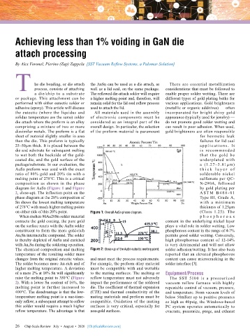
        diagram for AuSn (Figure 1 and Figure                                                  by gold plating per
        2, close-up). The inflection point on the                                              A S T M B 48 8 - 01
        phase diagram at the 20% composition of                                                Type III, Grade A,
        Sn shows the lowest melting temperature                                                with a minimu m
        of 278°C with much higher melting points                                               thickness of 1.25µm
        on either side of this 20% point.  Figure 1: Overall AuSn phase diagram.               (Class 1.25). The
          When molten 80Au20Sn solder material                                                 ph o s ph o r ou s
        contacts the gold coating, the pure gold                              content in the underlying nickel layer
        on the surface reacts with the AuSn solder                            plays a vital role in solder wetting. Low
        constituent to form the more gold-rich                                phosphorous content in the range of 4-7%
        Au 5 Sn intermetallic compound. The solder                            permits good solder wetting. Conversely,
        is thereby depleted of AuSn and enriched                              high phosphorous content of 12-14%
        with Au 5 Sn during the soldering operation.                          is very detrimental and will not allow
        The chemical composition and melting   Figure 2: Close-up of the AuSn eutectic melting point.  solder adhesion/wetting. It has also been
        temperature of the resulting solder mass                              reported that an elevated phosphorous
        changes from the original eutectic values.   and must meet the process requirements.   content can cause microcracking in the
        The solder becomes more Au-rich and of   For example, the preform alloy material   solder interface [3].
        higher melting temperature. A deviation   must be compatible with and wettable
        of a mere 2% at 18% Sn will significantly   to the mating surfaces. The melting or   Equipment/Process
        raise the melting point to 350°C (Figure    reflow temperature must not adversely   The SST 5100 is a pressur ized
        2). With a lower Sn content of 16%, the   impact the performance of the soldered   vacuum  reflow  furnace  with highly
        melting point is further increased to   die. The coefficient of thermal expansion   repeatable control of vacuum, pressure,
        400°C. The disadvantage is that the low-  (CTE) and thermal conductivity of the   and temperature. From vacuum levels of
        temperature melting point is a one-time-  mating materials and preform must be   below 50mTorr up to positive pressures
        only reflow; a subsequent attempt to reflow   compatible. Oxidation of the mating   as high as 40psig, the Windows-based
        this solder would require a much higher   surfaces is very critical, especially for   PC system operates automatically to
        reflow temperature. The advantage is that   non-gold surfaces.        evacuate, pressurize, purge, and exhaust


        26   Chip Scale Review   July  •  August  •  2020   [ChipScaleReview.com]
        26

