Page 27 - ChipScale_Jul-Aug_2020-Digital
P. 27
the die cut out the sinter film to the exact   References
                                           die size, at which point the die is then   1.  A. Fahim, S. Ahmed, M. Mahmudur,
                                           extracted together with the laminated   R. Chowdhury, J. C. Suhling, P.
                                           sinter material. The die is subsequently   Lall, “High- temperature creep
                                           tacked or in situ sintered onto the heated   response of lead-free solders,” 15th
                                           substrate. A cross section of the resultant   IEEE Intersociety Conf. on Thermal
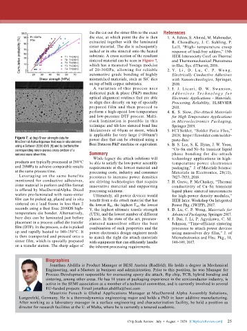
                                           sintered material can be seen in Figure 7,   and Thermomechanical Phenomena
                                           which has a measured Youngs modulus    in Elec. Sys. (ITherm), 2016.
                                           of 20-30GPa, allowing for reliable   2.  Y.   L i ,  D.  L u ,  C .  P.   Wo n g ,
                                           automotive grade bonding of highly     Electrically Conductive Adhesives
                                           mismatched materials, such as SiC dies   with Nanotechnologies, Springer,
                                           on top of bulk copper substrates.      2010.
                                             A variation of this process uses   3.  J.  J.  Licar i,  D.  W.  Swanson,
                                           dedicated pick & place (P&P) machine   A d h e si v e s Te c h n o l o g y  f o r
                                           optical alignment routines that are able   Electronic Applications – Materials,
                                           to align dies directly on top of specially   Processing, Reliability,  ELSEVIER
                                           prepared film and then proceed to      2011.
                                           perform a high-speed low-temperature   4.  K. S. Siow, Die-Attach Materials
                                           and low-pressure DTF process. Multi-   for High Temperature Applications
                                           stack  lamination  is  possible  in  this   in Microelectronics Packaging,
                                           technique and tilt-less sintered bond line   Springer 2019.
                                           thicknesses of 60µm or more, which   5.  FCTSolder, “Solder Paste Flux,”
                                           is applicable for very large (>100mm²)   2018; https://fctsolder.com/solder-
        Figure 7: a) (top) Shear strength data for   power dies that can be obtained using a   paste-flux/
        MacDermid Alpha Argomax that was in situ sintered   Besi Datacon P&P machine or equivalent.
        using a Datacon 2200 EVO [9] and b) (bottom) the                        6.  B. S. Lee, S. K. Hyun, J. W. Yoon,
        corresponding micro-porous cross section of a                             “Cu–Sn and Ni–Sn transient liquid
        sintered nano silver film.         Summary                                phase bonding for die-attach
                                             While legacy die attach solutions will   technology applications in high-
        products are typically processed at 280°C   be able to satisfy the low-power assembly   temperature power electronics
        and 20MPa to achieve comparable results   requirements at the lowest material and   packaging,”  J. of Materials Science:
        at the same process time.          processing costs, industry and consumer   Materials in Electronics, 28(11),
          Leveraging on the same benefits   pressures to increase power densities   7827–7833, 2016.
        mentioned for conductive adhesives,   are driving technologies that require   7.  H. Greve, P. McCluskey, “Thermal
        sinter material in preform and film format   innovative material and supporting   conductivity of Cu-Sn transient
        is offered by MacDermidAlpha. Diced   processing solutions.               liquid phase sintered interconnects
        wafers pre-laminated with nano-sinter   Ultimately, all power devices would   for high-power density modules,”
        film can be picked up, placed and in situ   benefit from a die attach material that has   IEEE Inter. Workshop On Integrated
        sintered on a lead frame in less than 2   the lowest R th , the highest T M , the lowest   Power Pkg. (IWIPP), 2017.
        seconds using a Besi Esec 2100DS high-  Y, the highest ultimate tensile strength   8.  D. Lu, C. P. Wong, Materials for
        temperature die bonder. Alternatively,   (UTS), and the lowest number of different   Advanced Packaging, Springer 2017.
        bare dies can be laminated just before   phases. In the state of the art, pressure-  9.  J. Dai, J. Li, P. Agyakawa, C. M.
        placement in a process called die transfer   sintered nanosilver offers the best   Johnson, “Time-efficient sintering
        film (DTF). In the process, a die is picked   combination of such properties and the   processes to attach power devices
        up and rapidly heated to 140-150°C. It   power electronics design engineer needs   using nanosilver dry film,” J. of
        is then transported and pressed onto a   to match the right die attach materials   Microelectronics and Elec. Pkg., 14,
        sinter film, which is specially prepared   with equipment that can efficiently handle   140-149, 2017.
        on a transfer station. The sharp edges of   the inherent processing requirements.


                       Biographies
                         Jonathan Abdilla is Product Manager at BESI Austria (Radfeld). He holds a degree in Mechanical
                       Engineering, and a Masters in business and administration. Prior to this position, he was Manager for
                       Process Development responsible for overseeing epoxy die attach, flip chip, TCB, hybrid bonding and
                       sintering, among other areas. He has 14 years of packaging experience in the semiconductor industry, is
                       active in the SEMI association as a member of a technical committee, and is currently involved in several
                       EU-funded projects. Email jonathan.abdilla@besi.com
                         Maurizio Fenech is Global Applications Manager at MacDermid Alpha Assembly Solutions,
          Langenfeld, Germany. He is a thermodynamics engineering major and holds a PhD in laser additive manufacturing.
          After working as a laboratory manager in a surface engineering and characterization facility, he held a position as
          director for research facilities at the U. of Malta, where he is currently a tenured academic.


                                                                                                             25
                                                             Chip Scale Review   July  •  August  •  2020   [ChipScaleReview.com]  25

