Page 20 - ChipScale_Jul-Aug_2020-Digital
P. 20
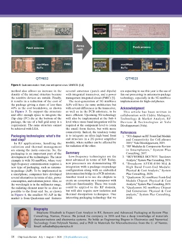
Figure 4: Qualcomm module: front, rear and opened views. SOURCES: [5,6]
        method also allows an increase in the   several antennas (patch and dipole)   are expecting to see this year is the use of   DELIVERS INDUSTRY LEADING PERFORMANCE
        density of the internal structure because   with integrated transceiver, and a power   fan-out processing in antenna-in-package
        the sensitive devices are outside. Finally,   management integrated circuit (PMIC) [5].   technology, especially in the 5G mmWave
        it results in a reduction of the cost of   The next-generation of 5G mmWave   implementation for high-end phones.
        the package giving a share of less than   AiPs will have the same architecture but
        40% in the cost breakdown, as shown   with several differences in the transceiver,   Acknowledgment
        in Figure 3. To support the structure   as well as in the PCB substrate, to be   This  article has  been  written  in
        and offer enough space to integrate the   more efficient. Upcoming 5G technology   collaboration with Cédric Malaquin,
        flip-chip (FC) die at the bottom of the   will also be implemented at the Sub-6   Technology  &  Market  Analyst,  RF
        package, the use of a ball grid array is a   level where more band integration will be   Devices  &  Tech nologies  at  Yole      Kulicke & So a’s Katalyst™ delivers the
        requirement. The same structure cannot   required at the component level to retain   Développement (Yole).
        be achieved with LGA.              the small form factor, but with more
                                           connectivity. Indeed, the tendency today   References                                  industry leading performance in accuracy and
        Packaging technologies: what’s the   is to integrate an ultra-high band front   1.  “5G’s Impact on RF Front-End Module
        next step?                         end structure in a 2G power amplifier   and Connectivity for Cell phones              speed for flip-chip placement. Its hardware and
          In RF applications, handling the   module, where neither can be affected by   2019,” Yole Développement, 2019.
        radiation and thermal management   the radiation of the other.          2.  “RF Modules & Components Review                       technology enable < 3 μm accuracy on
        are among the main concerns. So, the                                      in Smartphones,” System Plus
        packaging is an important part of the   Summary                           Consulting, 2017.
        development of the technologies. The latest   Low-frequency technologies are the   3.  “SKYWORKS SKY78191 Teardown                      substrate or wafer, o ering lower
        example is with 5G mmWave, where very   most advanced in terms of SiP. Today,   Analysis,” System Plus Consulting, 2019.
        high-frequency communication requires a   new processors are demonstrating 3D   4.  “Broadcom AFEM-8100 Mid &                         Cost-of-Ownership in the industry.
        new type of packaging, such as antenna-  integration with a package-on-package   High Band Front-End Module:
        in-package (AiP). To be implemented in   configuration along with an embedded   Physical & Cost Analysis,” System
        a smartphone, companies have developed   interconnection bridge in a PCB substrate.   Plus Consulting, 2020.
        several alternatives in terms of size, power   Another trend is to use die chiplets to   5.  “Qualcomm 5G mmWave Front-End
        consumption, and radiation power. Also, as   create an ecosystem on a transposer with   Module Chipset: Physical & Cost
        the wavelength is in the millimeter range,   different functionality. These two trends   Analysis,” System Plus Consulting, 2019.
        the radiating element must be as close as   could  be  applied  to  the  RF  domain,   6.  “Qualcomm 5G mmWave Chipset
        possible to the front end. So, as shown   but will also require new isolation and   2nd Generation: Physical & Cost
        in Figure 4, the smallest 5G AiP in the   thermal dissipation techniques. One   analysis,” System Plus Consulting,
        market is from Qualcomm and  features   interesting packaging technology that we   2020.


                       Biography
                         Stéphane Elisabeth is Expert Cost Analyst in RF, Sensors and Advanced Packaging at System Plus
                       Consulting, Nantes, France. He joined the company in 2016 and has a deep knowledge of materials
                       characterizations and electronics systems. He holds an Engineering Degree in Electronics and Numerical
                       Technology from Polytech Nantes, and a PhD in Materials for Microelectronics from the U. of Nantes.
                       Email: selisabeth@systemplus.fr


        18   Chip Scale Review   July  •  August  •  2020   [ChipScaleReview.com]
        18

