Page 15 - ChipScale_Jul-Aug_2020-Digital
P. 15
Besi Enables “More than Moore”


        further extend the panel-level packaging
        line with a couple of new equipment
        installations (Figure 4).
 The World Leader in Advanced   2020 based on a schedule of discussions
          The consortium launch was February
        and in consultation with an International
 Packaging Process Equipment  Advisory Board made up of industry leaders
        from Japan, Korea, Europe, and the U.S.
        A final executive summary was generated
        to send to companies around the world that
        are interested in joining the consortium
 ThermoCompression Bonding  and finalizing the initial research launch
        program based on the funds available from

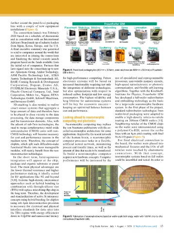
 •  Proven HVM TC Bonder  the initial set of companies. Partners that   Figure 4: Panel-level packaging line (457mm x 305mm, some machines are 600mm x 600mm) at Fraunhofer
        have signed onto the consortium up to now
        are: Ajinomoto Group, Amkor Technology,
                                           IZM in Berlin.
 •  8800 TC  Next  ASM Pacific Technology Ltd., AT&S   for high-performance computing. Future   use of specialized and reprogrammable
        Austria Technologie & Systemtechnik AG,
 •  Die size up to 70x70 mm  BASF, Corning Research & Development   electronic systems will be based on   processors, non-volatile memory circuits,
                                           increased functionality requiring not only
                                                                              high-speed optoelectronic or photonic
        Corporation, Dupont, Evatec AG,
 •  1.5mm, 3s accuracy  FUJIFILM Electronic Materials U.S.A.,   the integration of different technologies,   communication, and flexible self-learning
 m
 s
                                           but also optimization with respect to
                                                                              algorithms. Together with the Kirchhoff-
        Hitachi Chemical Company, Ltd., Intel
 •  Inert bonding ambient option  Corporation, Meltex Inc., Nagase, RENA   reduced carbon footprint and low energy   Institute for Physics, Fraunhofer IZM
                                           consumption. The highest reliability and
                                                                              has developed a full-wafer redistribution
        Technologies GmbH, Schmoll Maschinen,
                                           long lifetime for autonomous systems
                                                                              and embedding technology as the basis
 •  Superior Tilt Control  and Semsysco GmbH.  will be key for economic success—  for a large-scale neuromorphic hardware
          3D-stacking is also needed to realize
                                                                              system. In the first phase of the project,
                                           keeping an optimized balance between
        smart sensor systems that aggregate a
        large amount of data and therefore have   cost and performance.       standard redistribution technologies from
        to be placed in close vicinity to the data                            wafer-level packaging were adapted to
 Die to Wafer Hybrid Bonding  processing, the data storage components   Looking ahead to neuromorphic   enable a high-density reticle-to-reticle
                                                                              routing on 200mm CMOS wafers [11].
                                           computing and photonics
        and the transmission elements. Also, with
                                             Neuromorphic computing may replace
 •  8800 Chameo  ultra plus  the advent of sub-7nm technologies, the   the von Neumann architecture with the so-  Neighboring reticles of the CMOS chips
                                                                              on the wafer were interconnected using
        need to merge complementary metal oxide
                                                                              a polymer/Cu-RDL across the scribe
        semiconductor (CMOS) cores with non-
                                           called neuromorphic architecture for some
 •  Ultra High Accuracy C2W Bonder  CMOS technology will become necessary   applications. Inspired by the neural network   lines with an 8µm pitch routing with final
                                                                              Ni/Ai I/O-pads (Figure 5).
                                           of the human brain, a neuromorphic
        for cost and performance reasons in the
 •  Advanced Cleanliness by Design  medium term. Therefore, the concept of   computer processes tasks in a flexible,   the board, the wafers were placed into
                                                                                For  final  electrical  connection  to
        chiplets, which split such difficult-to-make
                                           artificial neural network, minimizing
 •  Highest Throughput  functional blocks into more manageable   process and transfer times, as well as the   mechanical fixtures and the I/Os of all
                                                                              reticles were touched by elastomeric
                                           amount of data that needs to be transferred.
        modules, will mainly benefit from the new
 •  200nm, 3s accuracy  interconnection technologies.  To build a neuromorphic computer   c o n n e c t o r s .  Wit h  t h a t  c o n c e p t ,
 s
                                                                              neuromorphic systems based on full wafers
                                           requires new hardware concepts. Computer
          In the short term, heterogeneous
 •  > 2000 CPH  integration will appear at the chip,   performance will be increased by the   could be assembled and tested. In order to
        package and organic substrate or panel
        level. The main physical advantages are
        the lower thermal resistance and higher
        performance making it ideally suited
        for RF applications like 5G and beyond
        [9,10]. Extreme high-density interconnect
        approaches such as hybrid bonding in
        combination with through-silicon vias
        (TSVs) will replace microbump flip-chip in
        the long term. Therefore, the development
        and standardization of active Si-interposer
        concepts using hybrid bonding for chiplets
        using sub-1µm interconnection precision
        is necessary for electrical and physical
        interface standards for data rates into
 www.besi.com  the TB/s regime with energy efficiencies
        down to 0.2pJ/bit and nanosecond latency
                                           Figure 5: Fabrication of neuronal networks based on wafer-scale technology: wafer with 159744 chip-to-chip
                                           connections (Fraunhofer IZM).
                                                                                                             13
                                                             Chip Scale Review   July  •  August  •  2020   [ChipScaleReview.com]  13

