Page 10 - ChipScale_Jul-Aug_2020-Digital
P. 10
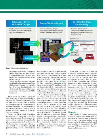
Figure 3: Integrated chiplet design flow.
            designing a single device to designing   for designing multi-chiplet-based   Fr om t he s ys t e m -level d e sig n
            and/or integrating multiple devices,   packages, starting with a single logical   framework discussed above, the user
            the requirement for defining and   hierarchical representation of the   should be able to design and/or import
            managing top-level connectivity   complete multi-chiplet design from the   multiple chips or chiplets across any
            becomes crucial.               transistor level of each chiplet up to   technology or node. The designer
          • Test is another area that changes  the full system-level design (Figure   would then instantiate each chiplet
            significantly when designing multiple  3). This system-level schematic is the   schematic symbol into the top system-
            chiplets in a 3D stack. For example,  basis for seamless LVS and functional   level schematic,  where additional
            how do you test the chiplet in the top  verification that ideally includes layout   package-/board-level  devices could
            of the stack that may not have any  parasitics across chiplets, interposers   easily be added from the system-
            connections to the outside world? The  and package substrates. It should even   level library. This schematic serves
            list goes on.                  extend to the PCB if the user desires.  multiple purposes, including system-
                                             A novel approach to chiplet/package   aware functional simulation, and
          The bottom line is that laying-out   co-design can also be enabled as   maybe most importantly, it provides the
        and verifying designs with multiple   part of this holistic, system-level   golden netlist required to perform LVS
        chiplets will introduce new challenges   design platform. Finally, multiple   checking of the complete system-level
        for both the IC design team, as well as   electromagnetic field solvers, including   design. This methodology provides the
        the package designers. Design tools and   finite element method (FEM) and   designer system-level signoff confidence
        methodologies that have been extended   method of moments (MoM), must   at the same level they have when signing
        to support multiple chiplets play a   be integrated in the f low, allowing   off on their individual chiplet.
        crucial role in the success or failure of   streamlined device modeling and layout
        your next project.                 parasitic extraction for both on-chiplet   Biography
          F r o m a n E DA t o o l p r o v i d e r   and off-chiplet geometries. There   John Park is the Product Management
        perspective, it’s important to develop   should be automation that seamlessly   Group Director for Advanced IC
        cross-domain design flows that provide   stitches the electrical models back   Packaging at Cadence, based in Boulder,
        users with a platform to seamlessly   into the golden hierarchical system-  CO. In this role, John leads a team
        plan, design, analyze and verify across   level schematic. Such a platfor m   focused on the development of advanced
        chiplet, interposer, package substrate,   would provide designers an easy way   semiconductor  packaging  and  IC/
        and board. This platfor m should   to transition into the world of chiplet-  package/PCB cross-platform solutions.
        provide many unique capabilities   based architectures.               Email jpark@cadence.com


        8 8  Chip Scale Review   July  •  August  •  2020   [ChipScaleReview.com]

