Page 20 - ChipScale_May-June_2020-digital
P. 20
Patterning modularity and vital    L/S result was achieved through further
                                           positioning in sub-grid            process optimization involving the reduction
                                             The resolution of MLE is aimed at typical   of surface reflection effects, which can be
                                           back end of line (BEOL) resolutions with   achieved by applying anti-reflective coatings
                                           fine control of the irradiated lines, as well as   or modifying substrate material properties.
                                           their gaps (L/S <2µm), while maintaining   The MLE technology can also finely
                                           critical  dimension (CD)  uniformity   control DoF in order to achieve steep
                                           (CDU<10% CD) and positional accuracy of   sidewalls,  thereby keeping the desired 3D
                                           any arbitrary structures considerably within   contour of the resist, or preventing edge
                                           the patterning grid scale. This precision   topping and footing. Large working distance
                                           is matched by the distortion-free optics   and automatic adaptive focus ensures
                                           and the stage placement accuracy, which   patterning uniformity across the exposure
                                           ensures seamless projection across the entire   surface. Commonly used TOK P-W1000T
                                           substrate. The exposure can be performed   resist for fine-line and core-line RDL
                                           flexibly with a very high degree of freedom   creation was chosen to demonstrate various
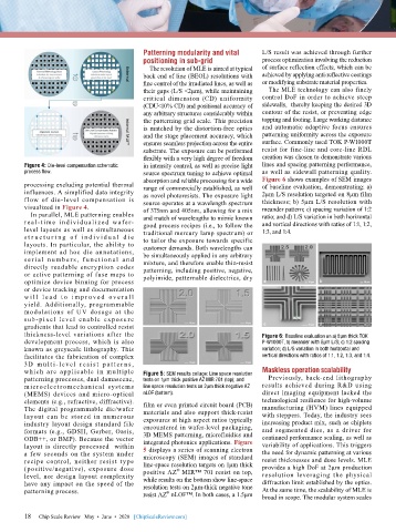
        Figure 4: Die-level compensation schematic   in intensity control, as well as precise light   lines and spacing patterning performance,
        process flow.                      source spectrum tuning to achieve optimal   as well as sidewall patterning quality.
                                           absorption and reliable processing for a wide   Figure 6 shows examples of SEM images
        processing excluding potential thermal   range of commercially established, as well   of baseline evaluation, demonstrating: a)
        influences. A simplified data integrity   as novel photoresists. The exposure light   2µm L/S resolution targeted on 8µm film
        f low of die-level compensation is   source operates at a wavelength spectrum   thickness; b) 5µm L/S resolution with
        visualized in Figure 4.            of 375nm and 405nm, allowing for a mix   meander pattern; c) spacing variation of 1:2
          In parallel, MLE patterning enables   and match of wavelengths to mimic known   ratio; and d) L/S variation in both horizontal
        re al-t i me i nd iv idu al i ze d wafe r-  good process recipes (i.e., to follow the   and vertical directions with ratios of 1:1, 1:2,
        level layouts as well as simultaneous   traditional mercury lamp spectrum) or   1:3, and 1:4.
        s t r u c t u r i ng o f i n d i v i d u a l d i e   to tailor the exposure towards specific
        layouts. In particular, the ability to   customer demands. Both wavelengths can
        implement ad hoc die annotations,   be simultaneously applied in any arbitrary
        s e r i a l nu m b e r s , f u n c t io n a l a n d   mixture, and therefore enable thin-resist
        directly readable encryption codes   patterning, including positive, negative,
        or active patterning of fuse maps to   polyimide, patternable dielectrics, dry
        optimize device binning for process
        or device tracking and documentation
        w i l l  l e a d t o i m p r o v e d o v e r a l l
        yield.  Additionally,  programmable
        modulations of UV dosage at the
        sub -pi xel level enable exposu re
        gradients that lead to controlled resist
        thickness-level variations after the                                  Figure 6: Baseline evaluation on a) 8µm thick TOK
        development process, which is also                                    P-W1000T, b) meander with 5µm L/S; c) 1:2 spacing
        known as greyscale lithography. This                                  variation; d) L/S variation in both horizontal and
        facilitates the fabrication of complex                                vertical directions with ratios of 1:1, 1:2, 1:3, and 1:4.
        3D m u l t i - l e vel r e s i s t p a t t e r n s ,
        which are applicable in multiple   Figure 5: SEM results collage: Line space resolution   Maskless operation scalability
        patterning processes, dual damascene,   tests on 1µm thick positive AZ MIR 701 (top); and   Previously, back-end lithography
        microelect romechanical systems    line space resolution tests on 2µm thick negative AZ   results achieved during R&D using
        (MEMS) devices and micro-optical   nLOF (bottom).                     direct imaging equipment lacked the
        elements (e.g., refractive, diffractive).   film or even printed circuit board (PCB)   technological resilience for high-volume
        The digital programmable die/wafer   materials and also support thick-resist   manufacturing (HVM) lines equipped
        layout can be stored in numerous   exposures at high aspect ratios typically   with steppers. Today, the industry sees
        industry layout design standard file   encountered in wafer-level packaging,   increasing product mix, such as chiplets
        formats (e.g., GDSII, Gerber, Oasis,   3D MEMS patterning, microfluidics and   and segmented dies, as a driver for
        ODB++, or BMP). Because the vector   integrated photonics applications. Figure   continued performance scaling, as well as
        layout is  directly processed  within   5 displays a series of scanning electron   variability of applications. This triggers
        a few seconds on the system under   microscopy (SEM) images of standard   the need for dynamic patterning at various
        recipe control,  neither  resist  type   line-space resolution targets on 1µm thick   resist thicknesses and dose levels. MLE
        (positive/negative), exposure dose   positive AZ  MIR™ 701 resist on top,   provides a high DoF at 2µm production
                                                     ®
        level, nor design layout complexity   while results on the bottom show line-space   resolution leveraging the physical
        have any impact on the speed of the   resolution tests on 2µm-thick negative tone   diffraction limit established by the optics.
        patterning process.                resist AZ  nLOF™. In both cases, a 1.5µm   At the same time, the scalability of MLE is
                                                  ®
                                                                              broad in scope. The modular system scales
        18   Chip Scale Review   May  •  June  •  2020   [ChipScaleReview.com]
        18

