Page 31 - Chip Scale Review_November-December_2023-digital
P. 31
High-speed probe card architecture for high-end devices


        By Xin-Reng Foo, Chee Hoe Lin  [AMD Singapore]  Alberto Berizzi [TECHNOPROBE Italy]

        D          e m a n d  f or  a r t i f i ci a l   Leveraging of advanced packaging   complicated process. The standard


                   i n te ll i g en c e  ( A I ) ,
                                                                              meet all HPC testing requirements
                   m a c h i n e l e a r n i ng   used in chiplets technology is driving   probe card solutions are not able to
                                           demand for on-chip interconnect
        (ML), high-performance computing   between the computing cores, I/Os   inclusive of high-speed I/O (HSIO),
        ( H PC), hy p e r sca le d at a c e nt e r s   and memory controllers (MCs). For   high current-carrying capacity and
        and Cloud comput i ng has led to   next-generation devices, developers   high insertion count. The bump pattern
        a rapid development of advanced    are driving even greater computing   of a HSIO system on chip (SoC)
        technologies. These technologies   power, higher resolution graphics,   block from an IP vendor is often not
        allowed the processing of a high-  a nd i mprove d me d ia proce ssi ng   optimized for signal integrity that may
        volume of data as well  as solving   into the integrated chips that enable   contribute to impedance mismatches
        complex and performance-intensive   t h e s e s y s t e m s . T h i s h ig h l e vel   at the transitions from wafer to probe
        problems. This changes the overall   of integration is causing on-chip   head and probe card. These impedance
        landscape of product development   com mu nications  and  t ransaction   mismatches cause ref lection that
        by  enabling  a  faster  time  to  market   h a n d l i ng t o b e c o m e a s y s t e m   affect signal quality at the transceiver
        and a short prototyping cycle while   const r ai nt, t hereby li m it i ng t he   a n d r e c e ive r. Ad d it io n a l ly, t h e
        maintaining  control  of  the  overall   achievable performance of multi-die   combination of channel loss, signal
        p r o d uc t  de velo pm e nt  c o st .  T h e   packaging regardless of the level of   to noise ratio (SNR), and cross talk
        global HPC market was valued at    optimization of the individual central   will impact the channel performance.
        US$ 41.22 billion in 2022 and is   processing units (CPU), graphics   Eye diagram, S-parameters and time
        expected to hit around US$ 85.34   processing units (GPU), and other   domain ref lectometry (TDR) plots
        billion by 2032; it is poised to grow   intellectual property (IP) blocks [4].   are some of the ways to assess probe
        at a compound annual growth rate   This rapid development of technology   card SI figures of merit. It is possible
        (CAGR) of 7.6% during the forecast   pushes the requirement for high-end   to optimize a probe card design by
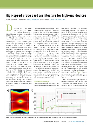
        per iod 2023 to 2032 [1]. Nea rly   probe cards, specifically in terms of   analyzing these plots. Figure 1 shows
        every company in the Fortune 100   meeting the ever-increasing speed   an  example  of  a  closed  eye  due  to
        list uses HPC, and its popularity is   requirement for reliable, high-speed,   probe card impedance mismatches at
        increasing at a rapid rate. Some of   and low-latency interconnects.  25GT/s.
        the industries using HPC include                                        Sort  hardware  design  sign  off  is
        aerospace, manufacturing, finance   Sort hardware design              mainly based on simulation data.
        technology (Fintech), healthcare, and   Achieving  design  targets  in  sort   Therefore, discrepancies  may exist
        retail [2-3].                      hardware design is a challenging and   between design expectations and the


        Figure 1: a) (left) Closed eye at NRZ 25GT/s; and b) (right) TDR plot of probe card signal path from the device under test (DUT) to the tester channel.

                                                                                                             29
                                                       Chip Scale Review   November  •  December  •  2023   [ChipScaleReview.com]  29

