Page 33 - Chip Scale Review_November-December_2023-digital
P. 33

t o d e velo p a h ig h - p e r fo r m a n c e   Sort hardware optimization   The following sections describe
        probe card that meets the design     Figure 2 shows the main design   the development and characterization
        requirements. This learning could be   challenges for a high-end probe card for   processes of new probe technology
        applied for future designs.        HPC applications and the development   dedicated to addressing high-speed
                                           process flow formulated by the authors.  performance. This new technology needs
                                                                              to be compliant with both new high-speed
                                                                              performance requirements for advanced
                                                                              chip-to-chip interconnects and other
                                                                              challenges required by high-end devices
                                                                              like high current carrying capacity, force
                                                                              control, lifetime, and so on.
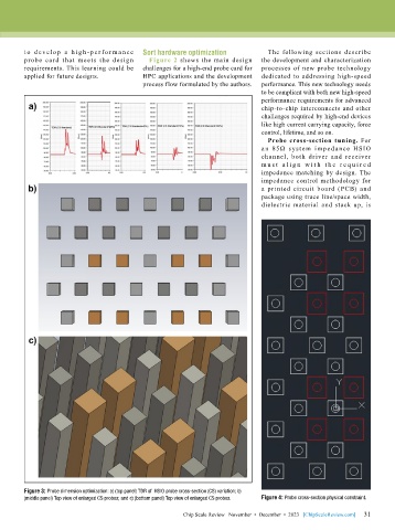
                                                                                Probe cross-section tuning. For
                                                                              an  85Ω  system  i mped ance  HSIO
                                                                              channel, both driver and receiver
                                                                              m u s t  a l i g n w i t h t h e  r e q u i r e d
                                                                              impedance matching by design. The
                                                                              impedance control methodology for
                                                                              a printed circuit board (PCB) and
                                                                              package using trace line/space width,
                                                                              dielectric material and stack up, is


        Figure 3: Probe dimension optimization: a) (top panel) TDR of  HSIO probe cross-section (CS) variation; b)
        (middle panel) Top view of enlarged CS probes; and c) (bottom panel) Top view of enlarged CS probes.  Figure 4: Probe cross-section physical constraint.

                                                                                                             31
                                                       Chip Scale Review   November  •  December  •  2023   [ChipScaleReview.com]  31
   28   29   30   31   32   33   34   35   36   37   38