Page 30 - Chip Scale Review_November-December_2023-digital
P. 30
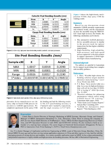
Figure 4 shows the high-density multi-
                                                                              junction VCSEL chip epoxy COB die
                                                                              bonding results.
                                                                              Summary
                                                                                Based on our discussions about
                                                                              automotive LiDAR assembly requirements
                                                                              and technical trends, and the experiments
                                                                              on laser die assembly using the MRSI-H-
                                                                              LD 1.5µm high-accuracy die bonder, the
                                                                              following conclusions can be drawn:

                                                                                1.  The automotive LiDAR photonics
                                                                                  device assembly process is similar
                                                                                  to the process used for optical
                                                                                  transceivers but has higher reliability
                                                                                  requirements.
        Figure 3: 905nm EEL high power laser die bonding results by eutectic and epoxy processes.  2.  High-flexibility, high-reliability,
                                                                                  high-accuracy, and high-speed
                                                                                  process equipment is the best solution
                                                                                  to support automotive LiDAR high-
                                                                                  mix/high-volume manufacturing.

                                                                              Acknowledgment
                                                                                The authors are grateful to Lumentum
                                                                              for its support in providing laser samples
                                                                              and assembly guidance.

                                                                              References
                                                                                1.  L. Zhou, “Flexible high-volume die
                                                                                  bonding solution targets modern
                                                                                  photonics manufacturing,” Laser
                                                                                  Focus World, July 2020.
                                                                                2.  P. E. Ross, “Aeva unveils Lidar on a
                                                                                  chip: Aeva says its high-performance
                                                                                  lidar will sell for less than US $500;
                                                                                  VW is buying it,” IEEE Spectrum,
                                                                                  Dec. 11, 2019.
                                                                                3.  “Practical solutions for enhancing
                                                                                  autonomous vehicle safety using
        Figure 4: High-density multi-junction VCSEL chips epoxy COB bonding results.  L i DA R- b a s e d 3D s e n s i n g ,”
                                                                                  Lumentum white paper, 2020.
        photonics device manufacturers use the   die bonding and had the following results:
        epoxy chip on board (COB) process for   1) The X/Y post-bonding accuracy is   4.  “Valeo Scala Laser Scanner Report,”
        automotive LiDAR applications. We   1.9μm@3σ and 1.3μm@3σ, respectively,   System Plus Consulting 2019.
        completed experiments for the epoxy COB   and the angle accuracy is 0.17°@3σ.   5.  “LiDAR for Automotive 2023
                                                                                         ©
                                                                                  Report,”  Yole Intelligence 2023.

                       Biographies
                         Limin Zhou is Senior Director of Strategic Marketing at MRSI Systems, Mycronic Group, and General
                       Manager of MRSI Automation (Shenzhen) Co., Ltd., Shenzhen, China. Prior to joining the company in
                       2019, he was Senior R&D Director at NeoPhotonics, China, NPI & Product Engineering Director in Oclaro
                       Asia, and NPI Operation Director in both JDSU and SAMN-SCI (China). He also worked at Sebit as co-
                       founder of a start-up laser company. His career began at Chartered Semiconductor (Singapore). He has a
                       PhD in Automation from Xi’an Jiaotong U. (XJTU). Email limin.zhou@mycronic.com

            Avy Yi is Senior Manager of Application and Service Engineering at MRSI, a part of Mycronic Group, Shenzhen, China. He
          joined MRSI 20 years ago and has been serving various application customers in China and other regions in Asia, familiar with the
          packaging process of various devices and modules. As a senior assembly application expert at MRSI, he has a deep understanding
          and practical experience in highly reliable and high-precision die bonding processes. He has a BE in Mechanical Engineering.


        28   Chip Scale Review   November  •  December  •  2023   [ChipScaleReview.com]
        28

