Page 15 - Chip Scale Review_September-October_2023-digital
P. 15
Many wafers cannot be tested at all using   be tested with two insertions: you test one   wafer dies: instead of moving the wafer
        standard prober architectures that involve   side first, then you flip the wafer and test   under a probe card that is docked to the
        a wafer prober where the wafer is docked   the opposite side. Conversely, a wafer with   tester—as it is commonly done on every
        on a chuck, and a probe card that is docked   pass-through dies cannot be tested at all.  test floor—we have developed a prober
        to the tester positioned on the top of the   To enable the adoption of these   architecture able to move multiple mobile
        wafer. If you have uneven geometries on   technologies and designs,  new test   probe cards over the wafer surface. This
        the wafer, the conventional way of probing   methodologies are being developed to   new technology combines our experience
        the wafer with a probe card is not viable   leverage probing technologies that enable   in both flying probe technology and mixed-
        because the probe card requires all the dies   higher parallelism and lower the cost of   signal testing. With this new technology,
        with the same shape and orientation. If you   test, while meeting the rapidly evolving   up to eight different small probe cards (four
        have different dies with different shapes on   technical challenges posed by trends in IC   on the top, and four on the bottom side)
        a MPW, you also cannot use a traditional   design and manufacturing.  can be equipped simultaneously on our
        prober unless you change the probe card                               TH2000 prober. Each one is mounted on
        to test different parts of the wafer with   Overturning the concept of probing  an independent robotic axis that moves in
        multiple insertions. As for the wafers that   An alternative approach to probing   the X, Y and Z directions (Figure 4).
        have dies mounted on both sides, they can   consists in inverting the way you probe
                                                                              Testing wafers with varied
                                                                              geometries
                                                                                Each of the eight probe cards on our
                                                                              new prober can have a different design,
                                                                              adapting to different die shape or pitch,
                                                                              including unconventional and high-
                                                                              density geometries. This design feature
                                                                              extends the range of applications that can
                                                                              be fully tested at the wafer level.
                                                                                With a single prober insertion, it is
                                                                              possible to: 1) perform both control
                                                                              pattern test and pad test; 2) test MPWs,
                                                                              dedicating a probe card to each specific
                                                                              device layout; and 3) test wafers with
                                                                              uneven geometries (e.g., with mirrored
                                                                              or rotated layout for the different dies).
                                                                              In all these cases, each probe card fulfills
                                                                              a specific test function, with a proper
                                                                              probing layout, working on the whole
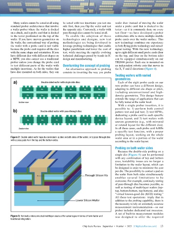
        Figure 2: Double-sided wafer layouts can include: a) dies on both sides of the wafer; or b) pass-through dies   wafer area or in a portion of the wafer
        with access pads from the top and the bottom sides.                   according to the wafer layout.

                                                                              Probing on both wafer sides
                                                                                Because the double-side probing on a
                                                                              single die (Figure 5) can be performed
                                                                              with any combination of top and bottom
                                                                              axes, testability issues are no longer a
                                                                              limitation to the wafer layout, which can
                                                                              be designed in order to minimize the cost
                                                                              per die. The possibility to contact a pad on
                                                                              the wafer from both sides simultaneously
                                                                              enables several limitations to be
                                                                              overcome. For example, continuity testing
                                                                              of pass-through dies becomes possible, as
                                                                              well as testing of multi-layer wafers (top-
                                                                              top, bottom-bottom, top-bottom), and also
                                                                              “virtual known-good die (KGD) testing.”
                                                                              All these test operations  imply that in
                                                                              addition to the probing capability, there is
                                                                              the necessity to rely on extremely accurate
                                                                              measurement instrumentation—so our
                                                                              prober includes dedicated test resources.
                                                                              A set of built-in measurement modules
        Figure 3: Vertically-interconnected multilayer stacks offer advantages in terms of form factor and   was  designed  to  offer  the  required
        functional integration.

                                                                                                             13
                                                         Chip Scale Review   September  •  October  •  2023   [ChipScaleReview.com]  13

