Page 16 - Chip Scale Review_September-October_2023-digital
P. 16
512A). For testing digital devices with a   and precise control of the effects of
                                           short distance between the pads, vertical   process variations. To cross-check the
                                           probes and wiring probes offer better   manufacturing process goodness and
                                           performance because they can work with   validate the reliability of the verification
                                           pitches of a few tens of micrometers.  pattern tests, top-bottom capacitive and
                                                                              resistive tests should be performed on
                                           Testing multi-layer stacked wafers  every chip, in addition to the kelvin tests
                                             As we have seen, vertical integration   performed on the verification patterns.
                                           is very effective as a way to reduce the   To keep under control every phase of the
                                           chip form factor while increasing the   process, this same test sequence should
                                           device functionality Looking closer, we   be repeated as every layer of the structure
                                           observe that multi-layer silicon wafer   is added.
                                           layouts often include verification patterns   The prober architecture based on
                                           in addition to the device dies. These   multiple mobile probe cards can be used
                                           patterns are meant to simplify the volume   to satisfy the test requirements noted
                                           production test of the devices because   above, during both the characterization
                                           the quality of the wafer can be validated   phase and the volume manufacturing
                                           through a kelvin test performed on the   phase. The same prober can mount—
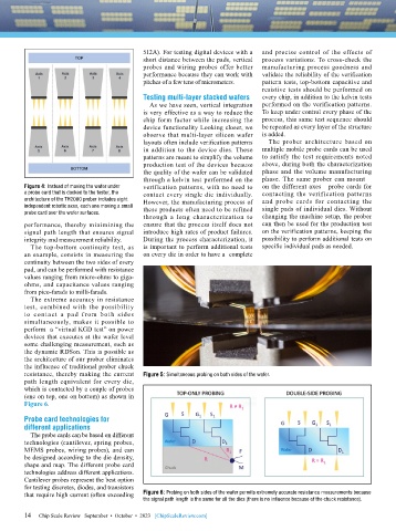
        Figure 4: Instead of moving the wafer under   verification patterns, with no need to   on the different axes—probe cards for
        a probe card that is docked to the tester, the   contact every single die individually.   contacting the verification patterns
        architecture of the TH2000 prober includes eight   However, the manufacturing process of   and probe cards for contacting the
        independent robotic axes, each one moving a small   these products often need to be refined   single pads of individual dies. Without
        probe card over the wafer surfaces.
                                           through a long characterization to   changing the machine setup, the prober
        performance, thereby minimizing the   ensure that the process itself does not   can then be used for the production test
        signal path length that ensures signal   introduce high rates of product failures.   on the verification patterns, keeping the
        integrity and measurement reliability.  During the process characterization, it   possibility to perform additional tests on
          The top-bottom continuity test, as   is important to perform additional tests   specific individual pads as needed.
        an example, consists in measuring the   on every die in order to have a  complete
        continuity between the two sides of every
        pad, and can be performed with resistance
        values ranging from micro-ohms to giga-
        ohms, and capacitance values ranging
        from pico-farads to milli-farads.
          The extreme accuracy in resistance
        test, combined with the possibility
        to contact a pad from both sides
        simultaneously, makes it possible to
        perform  a “virtual KGD test” on power
        devices that executes at the wafer level
        some challenging measurement, such as
        the dynamic RDSon. This is possible as
        the architecture of our prober eliminates
        the influence of traditional prober chuck
        resistance, thereby making the current   Figure 5: Simultaneous probing on both sides of the wafer.
        path length equivalent for every die,
        which is contacted by a couple of probes
        (one on top, one on bottom) as shown in
        Figure 6.
        Probe card technologies for
        different applications
          The probe cards can be based on different
        technologies (cantilever, spring probes,
        MEMS probes, wiring probes), and can
        be designed according to the die density,
        shape and map. The different probe card
        technologies address different applications.
        Cantilever probes represent the best option
        for testing discretes, diodes, and transistors
        that require high current (often exceeding   Figure 6: Probing on both sides of the wafer permits extremely accurate resistance measurements because
                                           the signal path length is the same for all the dies (there is no influence because of the chuck resistance).

        14
        14   Chip Scale Review   September  •  October  •  2023   [ChipScaleReview.com]

