Page 19 - Chip Scale Review_September-October_2023-digital
P. 19
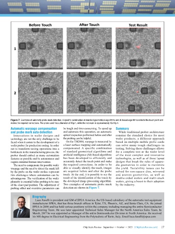
Figure 7: Examples of automatic probe mark detection. A specific combination of standard geometrical algorithms and AI-based algorithms detects the touch point and
        makes the required corrections. The probe used has a diameter of 20µm, while the red mark is approximately 16x12µm.
        Automatic warpage compensation     be tough and time-consuming. To speed up   Summary
        and probe mark auto detection      and automate this operation, an automatic   While traditional prober architecture
          Innovations  in  wafer  designs  and   optical inspection performed before and after   remains the standard choice for most
        technology are not the only challenge to be   the probing can be helpful.  wafer products, a different approach
        faced when it comes to the development of a   On the TH2000, warpage is measured by   based on multiple mobile probe cards
        wafer prober for production testing. In order   a laser surface mapping and automatically   can solve many tough challenges in
        not to transform testing operations into a   compensated. A specific combination   testing. Solving these challenges allows
        bottleneck in the manufacturing process, the   of standard geometrical algorithms and   for a complete test at the wafer level
        prober should embed as many automation   artificial intelligence (AI)-based algorithms   of the most complex and innovative
        features as possible and be autonomous and   has been developed to efficiently and   technologies, as well as of those layout
        require minimal human intervention.  accurately detect the touch point and make   designs that break the rules of square-
          The need to compensate for possible wafer   the required corrections. In order to be   die geometries in order to maximize
        warpage and the need to detect the mark left   able to visually identify the touch, images   the yield. Testability issues can be
        by the probe on the wafer surface represent   are acquired before and after the probe   solved for non-square dies, mirrored
        two challenges where automation can be   touch. At the end, it is possible to see the   and uneven geometries, as well as
        advantageous. The verification of the wafer   result of the identification of the touch by   double-sided wafers and multi-stack
        planarity is essential before probing to be sure   the developed image processing algorithm.   wafers, giving a boost to their adoption
        of the exact pad position. The adjustment of   Two examples of automatic probe mark   by the industry.
        probing offset and overdrive parameters can   detection are shown in Figure 7.

                       Biography
                         Luca Fanelli is president and GM of SPEA America, the US-based subsidiary of the automatic test equipment
                       manufacturer SPEA, that has three branch offices in Tyler, TX, Phoenix, AZ, and Santa Clara, CA. He joined
                       SPEA in 2006 and has held various positions within the company including managing the entire Semiconductor
                       Engineering Team. He was later appointed Technical Sales Manager for the North America Sales Team. In
                       March, 2017 he was appointed as Manager of the entire Semiconductor Division in North America. He received
                       his MS degree in Electrical Engineering from the Polytechnic of Turin, Italy. Email luca.fanelli@spea.com


                                                                                                             17
                                                         Chip Scale Review   September  •  October  •  2023   [ChipScaleReview.com]  17

