Page 24 - Chip Scale Review_September-October_2023-digital
P. 24
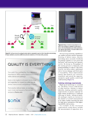
Figure 6: Measurements for every feature on six
                                                                              sides of the package are required at high-speed to
                                                                              ensure all critical dimensions are within specification.
                                                                              One capacitor here within all the solder balls is out of
                                                                              place and would be flagged.
        Figure 5: Sorting process for packaged semiconductor components based on defect inspection and metrology.   On-tool deep-learning capabilities
        AI-based solutions can provide additional speed and consistency for the best sorting accuracy.  can enable real-time smarter automatic
                                                                              bin ning of defect t y pes, thereby
                                                                              providing more accurate feedback
                                                                              on package quality to sort good and
                                                                              bad parts, and requiring less operator
                                                                              review. By doing so, throughput of
                                                                              the sorting process is improved, and
                                                                              manual handling is reduced. This latter
                                                                              benefit can help reduce additional
                                                                              risk of device damage and blind spots
                                                                              in traceability. These improvements
                                                                              ensure that defects are cor rectly
                                                                              identified and sorted for superior,
                                                                              automotive-grade quality control and
                                                                              yield learning (Figure 5).

                                                                              Evolving metrology requirements
                                                                                High-speed metrology is essential
                                                                              for checking cr itical dimensions
                                                                              of chip features. Similar to defect
                                                                              detection, meeting automotive quality
                                                                              requirements at speeds required for
                                                                              high-volume production is a difficult
                                                                              challenge to tackle. Advanced multi-
                                                                              die packages require an increase in
                                                                              the number of overall measurements
                                                                              to be taken, further stressing the need
                                                                              for high-speed automation with higher
                                                                              repeatability and accuracy.
                                                                                A n ex a m pl e of t h e i n c r e a s e d
                                                                              requirements noted above include
                                                                              the measurement of capacitors in a


        22   Chip Scale Review   September  •  October  •  2023   [ChipScaleReview.com]
        22

