Page 27 - Chip Scale Review_September-October_2023-digital
P. 27
Challenges with self-assembly applied to die-to-wafer


        hybrid bonding


        By Emilie Bourjot, Frank Fournel, Pierre Montméat, Loic Sanchez, Thierry Enot  [CEA-Leti]
        T        h e q u e s t f o r s m a l l e r   in  mass  production  especially  for   Today,  direct  placement  D2W  is


                 components with bet ter
                 performances at a competitive   imaging applications. In this approach,   performed by pick-and-place (P&P)
                                                                              processes that make it difficult to
                                           bonding is performed at wafer scale. With
        cost has been the driving force for   the latest generation of W2W bonders,   reconcile high placement accuracy with
        3D-IC (integrated circuit) technology   suppliers claim alignment capabilities of   high throughput. Indeed, to achieve
        developments for several decades.   less than 3σ. The main advantage of the   placement accuracy of better than
        Recent advances in bonding techniques   technique is high throughput. However,   1µm, P&P tool throughput must be
        have provided particular benefits for   there is a drawback in terms of design   lower than 1,000 dies per hour. Tool
        applications such as memory, high-  flexibility, which remains low because   suppliers are examining solutions to
        performance computing, and photonics,   the bottom and top dies must have the   increase this throughput, for example,
        where performance is strongly linked   same dimensions.               by implementing multiple heads on
        to the density of interconnections.   In contrast to W2W bonding, hybrid   P&P tools. However, breakthrough
        For such applications, hybrid bonding   D2W bonding should increase design   D2W processes are needed to remain
        emerged as a key booster to increase 3D   flexibility. This process re-uses the   competitive and to reach industrial
        interconnection density.           know-how developed for W2W, but    requirements. In this context, CEA-
          Hybrid bonding is similar to direct   adds dicing and cleanliness challenges.   Leti has been working for several years
        bonding except that it is applied to   When those challenges are managed,   on the development of a self-assembly
        mixed Cu/dielectric surfaces to create an   it will pave the way for heterogeneous   process. This promising process has
        electrical interconnection between two   3D structures by creating the means to   the potential to increase throughput to
        parts. Direct bonding is quite distinct   mix and match technologies on a single   several thousand dies per hour thanks
        from thermo-compression and adhesive   bottom substrate with high-density   to self alignment, and it is the subject of
        bonding, which require temperature and   interconnections. Moreover, the known-  this article.
        pressure, or additional materials such as   good die (KGD) concept can be applied
        polymer, respectively, to ensure contact   to increase overall product yield by   Self assembly driven by the
        between the two surfaces. In contrast,   selecting only good dies before assembly.   capillary forces of water droplets
        direct bonding is a spontaneous process,   D2W technology is of great interest for   The self-assembly process is based on
        and no external loading is required   many applications, such as edge devices   the use of the capillary forces of droplets
        during its thermal annealing step.   because of the increasing need for real-  of liquid to align a die to a target site on
        However, direct bonding does have   time computing of large amounts of data   a wafer. Capillary forces are exerted as
        stringent surface requirements in terms   with a limited power budget. Other “More   the liquid tries to minimize its surface
        of topography, planarity, roughness,   than Moore” applications are good   energy by regulating its surface tension.
        and particulate contamination. If   candidates, e.g., photonics, imagers and   From a macroscopic point of view, the
        uncontrolled, irregularities in these   displays, optical transceivers, and radio   liquid tends to minimize its interfacial
        characteristics can lead to bonding   frequency (RF).                 contact area with the surrounding air
        defects. The two critical parameters
        for successful direct bonding are clean
        surfaces and an appropriate topography.

        Direct hybrid bonding: W2W and
        D2W
          Two assembly configurations are
        possible with direct hybrid bonding:
        wafer-to-wafer (W2W) and die-to-wafer
        (D2W). W2W hybrid bonding was first
        proposed by Dr. Suga in 2000, then
        developed at CEA-Leti with hydrophilic
        bonding in 2009 in a R&D environment,
        and then Sony brought it to an industrial
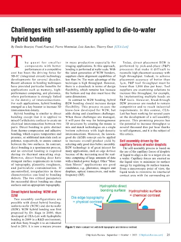
        level in 2016. It is now a mature process   Figure 1: Water containment with both topographic and chemical contrast.

                                                                                                             25
                                                         Chip Scale Review   September  •  October  •  2023   [ChipScaleReview.com]  25

