Page 30 - Chip Scale Review_September-October_2023-digital
P. 30
mechanisms. Therefore, it emerged
                                                                              that a weakly hydrophilic surface with
                                                                              a  water  contact  angle  (WCA)  >60°
                                                                              optimizes the collection and alignment
                                                                              of the dies. With 8x8mm² dies meeting
                                                                              this condition, excellent alignment yield
                                                                              with the mean alignment of x = 46nm
                                                                              and y = 132nm; 3σx = 439nm and 3σy
                                                                              = 341nm, along with a high throughput
                                                                              were obtained.
                                                                                In comparison, currently available die
                                                                              bonder P&P tools have achieved 1µm
                                                                              3σ, and the next generation of die bonder
                                                                              should reach 500nm 3σ. In addition to
                                                                              its very good alignment capability, the
                                                                              self-assembly process was demonstrated
                                                                              to behave like a “collective” process.
                                                                              After dicing, all dies were placed in a
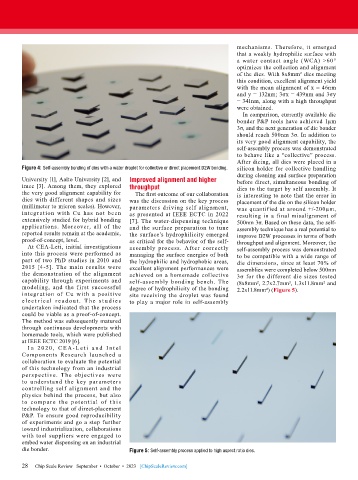
        Figure 4: Self-assembly bonding of dies with a water droplet for collective or direct placement D2W bonding.  silicon holder for collective handling
                                                                              during cleaning and surface preparation
        University [1], Aalto University [2], and   Improved alignment and higher   before direct, simultaneous bonding of
        imec [3]. Among them, they explored   throughput                      dies to the target by self assembly. It
        the very good alignment capability for   The first outcome of our collaboration   is interesting to note that the error in
        dies with different shapes and sizes   was the discussion on the key process   placement of the die on the silicon holder
        (millimeter to micron scales). However,   parameters driving self alignment,   was quantified at around +/-200µm,
        integration with Cu has not been   as presented at IEEE ECTC in 2022   resulting in a final misalignment of
        extensively studied for hybrid bonding   [7]. The water-dispensing technique   500nm 3σ. Based on these data, the self-
        applications. Moreover,  all of  the   and the surface preparation to tune   assembly technique has a real potential to
        reported results remain at the academic,   the surface’s hydrophilicity emerged   improve D2W processes in terms of both
        proof-of-concept, level.           as critical for the behavior of the self-  throughput and alignment. Moreover, the
          At CEA-Leti, initial investigations   assembly process.  After  correctly   self-assembly process was demonstrated
        into this process were performed as   managing the surface energies of both   to be compatible with a wide range of
        part of two PhD studies in 2010 and   the hydrophilic and hydrophobic areas,   die dimensions, since at least 70% of
        2015 [4-5]. The main results were   excellent alignment performances were   assemblies were completed below 500nm
        the demonstration of the alignment   achieved on  a homemade  collective   3σ  for  the  different  die  sizes  tested
        capability through experiments and   self-assembly bonding bench. The   (8x8mm², 2.7x2.7mm², 1.3x11.8mm² and
        modeling, and the first successful   degree of hydrophilicity of the bonding   2.2x11.8mm²) (Figure 5).
        integration of Cu with a positive   site receiving the droplet was found
        ele c t r ic a l r e a d ou t . T h e s t u d ie s   to play a major role in self-assembly
        undertaken indicated that the process
        could be viable as a proof-of-concept.
        The method was subsequently matured
        through continuous developments with
        homemade tools, which were published
        at IEEE ECTC 2019 [6].
          I n  20 20 ,  C E A- L e t i  a n d  I n t e l
        Components Research launched a
        collaboration to evaluate the potential
        of this technology from an industrial
        perspective. The objectives were
        to understand the key parameters
        controlling self alignment and the
        physics behind the process, but also
        to compare the potential of this
        technology to that of direct-placement
        P&P. To ensure good reproducibility
        of experiments and go a step further
        toward industrialization, collaborations
        with tool suppliers were engaged to
        embed water dispensing on an industrial
        die bonder.                        Figure 5: Self-assembly process applied to high aspect ratio dies.

        28
        28   Chip Scale Review   September  •  October  •  2023   [ChipScaleReview.com]

