Page 25 - Chip Scale Review_September-October_2023-digital
P. 25
then check overall position and tilt, while
                                                                              looking for any issues like cracks induced
                                                                              by the assembly process.
                                                                                As an industry, we’ve largely held a
                                                                              siloed view of front-end semiconductor
                                                                              processes, IC substrates and packaging.
                                                                              But as these technologies continue to
                                                                              evolve and overlap, we envision that shared
                                                                              learning will make it possible to implement
                                                                              new process control  strategies  for
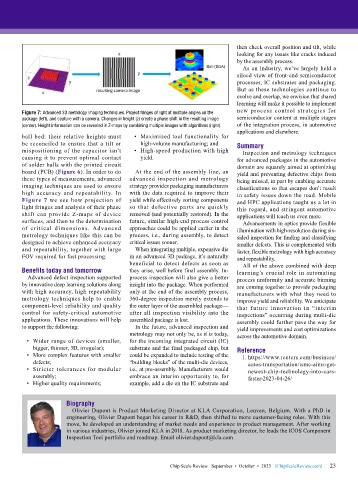
        Figure 7: Advanced 3D metrology imaging techniques. Project fringes of light at multiple angles on the
        package (left), and capture with a camera. Changes in height (z) create a phase shift in the resulting image   semiconductor content at multiple stages
        (center). Height information can be revealed in Z-maps by combining multiple images with algorithms (right).   of the integration process, in automotive
                                                                              applications and elsewhere.
        ball bed: their relative heights must   •  Maximized tool functionality for
        be reconciled to ensure that a tilt or   high-volume manufacturing; and  Summary
        mispositioning of the capacitor isn’t   •  High-speed production with high   Inspection and metrology techniques
        causing it to prevent optimal contact   yield.                        for advanced packages in the automotive
        of solder balls with the printed circuit                              domain are squarely aimed at optimizing
        board (PCB) (Figure 6). In order to do   At the end of the assembly line, an   yield and preventing defective chips from
        these types of measurements, advanced   advanced inspection and metrology   being missed, in part by enabling accurate
        imaging techniques are used to ensure   strategy provides packaging manufacturers   classifications so that escapes don’t result
        high accuracy and repeatability. In   with the data required to improve their   in safety issues down the road. Mobile
        Figure 7 we see how projection of   yield while effectively sorting components   and HPC applications taught us a lot in
        light fringes and analysis of their phase   so that defective parts are quickly   this regard, and stringent automotive
        shift can provide Z-maps of device   removed (and potentially restored). In the   applications will teach us even more.
        surfaces, and then to the determination   future, similar high-end process control   Advancements in optics provide flexible
        of  critical dimensions.  Advanced   approaches could be applied earlier in the   illumination with high-resolution during six-
        metrology techniques like this can be   process, i.e., during assembly, to detect   sided inspection for finding and classifying
        designed to achieve enhanced accuracy   critical issues sooner.       smaller defects. This is complemented with
        and repeatability, together with large   When integrating multiple, expensive die   faster, flexible metrology with high accuracy
        FOV required for fast processing.  in an advanced 3D package, it’s naturally   and repeatability.
                                           beneficial to detect defects as soon as   All of the above combined with deep
        Benefits today and tomorrow        they arise, well before final assembly. In-  learning’s crucial role in automating
          Advanced defect inspection supported   process inspection will also give a better   process uniformity and accurate binning
        by innovative deep learning solutions along   insight into the package. When performed   are coming together to provide packaging
        with high accuracy, high repeatability   only at the end of the assembly process,   manufacturers with what they need to
        metrology techniques help to enable   360-degree inspection merely extends to   improve yield and reliability. We anticipate
        component-level reliability and quality   the outer layer of the assembled package—  that future innovation in “interim
        control for safety-critical automotive   after all inspection visibility into the   inspections” occurring during multi-die
        applications. These innovations will help   assembled package is lost.  assembly could further pave the way for
        to support the following:            In the future, advanced inspection and   yield improvements and cost optimizations
                                           metrology may not only be, as it is today,   across the automotive domain.
          •  Wider range of devices (smaller,   for the incoming integrated circuit (IC)
            bigger, thinner, 3D, irregular);  substrate and the final packaged chip, but   Reference
          •  More complex features with smaller   could be expanded to include testing of the   1. https://www.reuters.com/business/
            defects;                       “building blocks” of the multi-die devices,   autos-transportation/tsmc-aims-get-
          •  Stricter tolerances for modular   i.e., at pre-assembly. Manufacturers would   newest-chip-technology-into-cars-
            assembly;                      embrace an interim opportunity to, for   faster-2023-04-26/
          •  Higher quality requirements;   example, add a die on the IC substrate and


                       Biography
                         Olivier Dupont is Product Marketing Director at KLA Corporation, Leuven, Belgium. With a PhD in
                       engineering, Olivier Dupont began his career in R&D, then shifted to more customer-facing roles. With this
                       move, he developed an understanding of market needs and experience in product management. After working
                       in various industries, Olivier joined KLA in 2018. As product marketing director, he leads the ICOS Component
                       Inspection Tool portfolio and roadmap. Email olivier.dupont@kla.com


                                                                                                             23
                                                         Chip Scale Review   September  •  October  •  2023   [ChipScaleReview.com]  23

