Page 13 - Chip Scale Review_September-October_2023-digital
P. 13
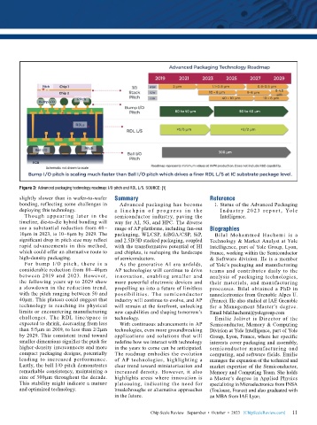
Figure 3: Advanced packaging technology roadmap: I/O pitch and RDL L/S. SOURCE: [1]
        slightly slower than in wafer-to-wafer   Summary                      Reference
        bonding, reflecting some challenges in   Advanced packaging has become   1.  Status of the Advanced Packaging
        deploying this technology.         a l i n c h p i n o f p r o g r e s s i n t h e   I n d u s t r y 2 0 2 3 r e p o r t , Yol e
          T houg h appea r i ng later i n the   semiconductor industry, paving the   Intelligence.
        timeline, die-to-die hybrid bonding will   way for AI, 5G, and HPC. The diverse
        see a substantial reduction from 40–  range of AP platforms, including fan-out   Biographies
        10µm in 2023, to 10–6µm by 2029. The   packaging, WLCSP, fcBGA/CSP, SiP,   Bilal Moham med Hachemi is a
        significant drop in pitch size may reflect   and 2.5D/3D stacked packaging, coupled   Technology & Market Analyst at Yole
        rapid advancements in this method,   with the transformative potential of HI   Intelligence, part of Yole Group, Lyon,
        which could offer an alternative route to   and chiplets, is reshaping the landscape   France, working within the Semiconductor
        high-density packaging.            of semiconductors.                 & Software division. He is a member
          For bu mp I /O pitch, there is a   As the generative AI era unfolds,   of Yole’s packaging and manufacturing
        considerable reduction from 80–40µm   AP technologies will continue to drive   teams  and contributes  daily to  the
        between 2019 and 2023. However,    innovation, enabling smaller and   analysis of packaging technologies,
        the following years up to 2029 show   more powerful electronic devices and   their materials, and manufacturing
        a slowdown in the reduction trend,   propelling us into a future of limitless   processes. Bilal obtained a PhD in
        with the pitch ranging between 50 and   possibilities. The semiconductor   nanoelectronics from Grenoble Alpes U.
        40µm. This plateau could suggest that   industry will continue to evolve, and AP   (France). He also studied at IAE Grenoble
        technology is reaching its physical   will remain at the forefront, unlocking   for a Management Master’s degree.
        limits or encountering manufacturing   new capabilities and shaping tomorrow’s   Email bilal.hachemi@yolegroup.com
        challenges. The RDL line/space is   technology.                         Emilie Jolivet is Director of the
        expected to shrink, decreasing from less   With continuous advancements in AP   Semiconductor, Memory & Computing
        than 5/5µm in 2019, to less than 2/2µm   technologies, even more groundbreaking   Division at Yole Intelligence, part of Yole
        by 2029. This consistent trend toward   applications and solutions that will   Group, Lyon, France, where her specific
        smaller dimensions signifies the push for   redefine how we interact with technology   interests cover packaging and assembly,
        higher-density interconnects and more   in the years to come can be anticipated.   semiconductor manufacturing and
        compact packaging designs, potentially   The roadmap embodies the evolution   computing, and software fields. Emilie
        leading to increased performance.   of AP technologies, highlighting a   manages the expansion of the technical and
        Lastly, the ball I/O pitch demonstrates   clear trend toward miniaturization and   market expertise of the Semiconductor,
        remarkable consistency, maintaining a   increased density. However, it also   Memory and Computing Team. She holds
        size of 300µm throughout the decade.   highlights areas where innovation is   a Master’s degree in Applied Physics
        This stability might indicate a mature   plateauing, indicating the need for   specializing in Microelectronics from INSA
        and optimized technology.          breakthroughs or alternative approaches   (Toulouse, France) and also graduated with
                                           in the future.                     an MBA from IAE Lyon.


                                                         Chip Scale Review   September  •  October  •  2023   [ChipScaleReview.com]  11 11

