Page 10 - Chip Scale Review_September-October_2023-digital
P. 10
thermal management, making them ideal   using an IC substrate to bridge the gap   of AI, 5G, and HPC applications. Specific
        for 5G devices.                    between the fan-out package and the   applications within 2.5D/3D stacked
          HPC. HPC applications, such as data   printed circuit board (PCB).  packaging include CIS using hybrid
        centers and supercomputers, require fast   Wafer-level chip-scale packaging   bonding technology, HBM for faster data
        and reliable processing. Technologies   (WLCSP). WLCSP involves packaging   access and improved memory bandwidth,
        such as fcCSP and FCBGA offer superior   ICs directly on a wafer, eliminating   3D-SoC for highly-integrated systems,
        electrical performance and higher    individual die singulation and packaging   and 3D NAND for increased storage
        I/O density, making them well-suited for   steps. The WLCSP offers compact form   density and capacity.
        HPC systems.                       factors, enhanced electrical performance,   System-in-package (SiP). SiP is a
                                           and cost efficiency, making it an ideal   type of AP that integrates multiple ICs,
        Exploring advanced packaging       choice for mobile devices and wearables,   or “chiplets,” into a single module. These
        platforms                          for which size, weight, and performance   chiplets,  which can  include  various
          The following sections describe major   are essential.              components like processors, memory,
        advanced packaging platforms.        fcBGA/CSP. These techniques involve   radio-frequency (RF) transceivers, and
          FO packaging. FO packaging includes   directly mounting ICs face-down onto   power management ICs, are interconnected
        three main categories: core fan-out,   organic substrates using solder micro-  within the package. This high level of
        high-density fan-out, and ultra high-  bumps or copper pillars. Flip-chip BGA/  integration allows a complete functional
        density FO. Core fan-out packaging   CSP solutions provide a smaller footprint,   system to be contained within a single
        eliminates the need for wire bonding   shorter interconnection paths, higher   package, making SiP a space-efficient
        or flip-chip interconnects, providing   I/O density, and improved electrical   solution perfect for applications where
        improved I/O density, enhanced electrical   performance than conventional wire-  form factor and integration are paramount,
        performance, and efficient thermal   bonded technology. These characteristics   such as mobile devices and wearables. SiP
        management. High-density (HD) FO   are especially critical in HPC applications   also offers significant flexibility in design
        takes the same concept further, employing   like servers, gaming consoles, and   and manufacturing, because each chiplet
        advanced redistribution layers (RDL) and   networking devices.        can be fabricated using the most suitable
        interconnect structures to achieve higher   2.5D/3D stacked packaging. 2.5D/3D   process technology for its function.
        I/O densities. Ultra high-density (UHD)   stacked packaging involves vertically
        FO uses finer-pitch and higher-density   stacking multiple dies or chips, creating a   Market shares and industry focus
        multi-layer RDLs for increased component   three-dimensional structure. This platform   The market for AP platforms is
        integration,  greater  bandwidth,  and   allows for higher integration levels,   witnessing significant growth, fueled
        advanced functionality within a compact   improved performance, and reduced   by the increasing demand for advanced
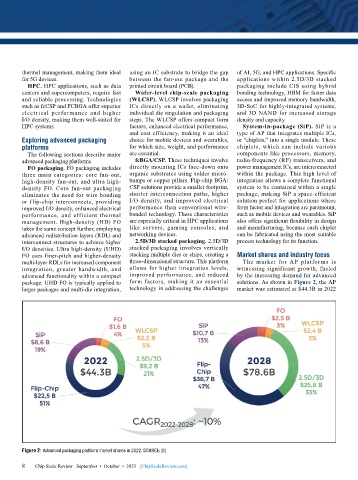
        package. UHD FO is typically applied to   form factors, making it an essential   solutions. As shown in Figure 2, the AP
        larger packages and multi-die integration,   technology in addressing the challenges   market was estimated at $44.3B in 2022


        Figure 2: Advanced packaging platform market shares in 2022. SOURCE: [1]

        8 8  Chip Scale Review   September  •  October  •  2023   [ChipScaleReview.com]

