Page 9 - Chip Scale Review_September-October_2023-digital
P. 9
MARKET TRENDS


                           Advanced packaging: Fueling the next era of


                           semiconductor innovation


                           By Bilal Mohammed Hachemi, Emilie Jolivet  [Yole Intelligence]

        T        oday, the semiconductor   methods, with different I/O density and   applications require high-performance


                                                                                A I and machi ne learning. A I
                                           I/O pitch depending on the targeted
                 industry is at the forefront
                 of technological innovation,
                 revolutionizing  var ious   application’s requirements, performance,   computing with low latency. AP platforms
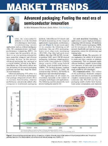
                                           and cost (Figure 1). In our recent report
                                                                              like 2.5D/3D stacked packaging, HBM,
        applications such as artificial intelligence   [1] we consider the following as AP   and Si interposers allow for higher
        (AI), 5G communications, and high-  platforms: fan-out (FO) packaging,   memory bandwidth and improved system
        performance computing (HPC). As    wafer-level chip-scale packaging   integration, critical for AI inference and
        we venture into the generative AI era,   (WLCSP), f lip-chip ball-grid array   training tasks.
        there is an ever-growing demand for   (fcBGA), flip-chip CSP (fcCSP), system-  Generative AI era. The generative AI
        more powerful, compact, and efficient   in-package (SiP), and 2.5D/3D stacked   era emphasizes the ability of AI models
        electronic devices. In this pursuit,   packaging, including complementary   to create new data, content, or solutions
        advanced packaging has emerged as   metal-oxide semiconductor (CMOS)   autonomously. This era demands highly
        a crucial enabler, pivotal in the More-  image sensors (CIS) using hybrid   efficient hardware capable of processing
        than-Moore era. This article delves into   bonding, high-bandwidth memory   vast amounts of data and generating
        the definition of advanced packaging   (HBM), 3D-stacked dynamic random   complex algorithms in real time, which is
        platforms and how they shape the future   access memory (DRAM) (3DS), 3D   made possible by AP technologies.
        of semiconductors.                 system-on-chip (3D-SoC), 3D NAND, Si   5G communication. The rollout
          Advanced packaging (AP) refers to a   interposers and embedded Si bridges.  of 5G technology demands compact
        diverse set of innovative technologies   The significance of AP cannot be   and efficient devices to accommodate
        that package integrated circuits (ICs)   overstated, especially in the context of   complex communication systems. AP
        to increase functionality, improve   emerging technologies and applications.   solutions like WLCSP and fan-out
        performance, and provide added value   The following sections present the main   packaging enable smaller form factors,
        compared to traditional packaging   drivers fueling the need for AP.  lower power consumption, and improved


        Figure 1: Advanced packaging technology roadmap: I/O density vs. I/O pitch. I/O density refers to total number of I/Os per package platform area. The plot was
        generated based on a Yole Group database, with reference to the industry average value. SOURCE: [1]

                                                         Chip Scale Review   September  •  October  •  2023   [ChipScaleReview.com]  7 7

