Page 25 - Chip Scale Review_May June_2023-digital
P. 25
Illumination inspection technology for defect detection


        on advanced IC substrates

        By Cheolkyu Kim, Burhan Ali, JungHyun Kim  [Onto Innovation]
        Jong Eun Park, Misun Hwang, Chan Jin Park, [Samsung Electro-Mechanics (SEMCO)]
        A          cross the semiconductor   potentially magnified as each new layer   material of epoxy polymer matrixes


                   industry, advanced integrated
                                           up. In some cases, the number of layers
                                                                              electrical properties of epoxy polymer can
                   circuit (IC) substrate (AICS)   of ABF on the FC-BGA substrate is built   and inorganic fillers. The chemical and
        supplies are low. The causes vary, from a   of build-up may reach 20. With each   be easily tailored by changing chemical
        limited number of suppliers who can meet   additional layer, the potential for killer   components to meet various material
        performance requirements, to constrained   defects increases, whether the cause is   requirements [1]. Another advantage of
        production capacities, and increased   ABF residue in laser-drilled vias, poor   ABF is that it facilitates the formation of
        demand resulting from the adoption of   dry-film resist development, or the under-   fine-pitch lines/spaces because its surface
        high-performance mobile devices, as well   and over-etching of Cu seed.  is receptive to laser processing and direct
        as advanced technologies like artificial   For  advanced  packaging  houses,   copper plating. This advantage, in part,
        intelligence (AI) and high-performance   addressing this issue is a matter of   makes ABF an ideal material for devices
        computing (HPC). And without question,   considerable interest. After all, few   where miniaturization is a driving force
        the ongoing shortage of Ajinomoto build-  businesses are not interested in reducing   for innovation. For pattern formation on
        up film (ABF), a necessary component   waste and cost, while more efficiently   the build-up layers of IC substrate, dry
        of many AICS, plays a significant role as   utilizing an in-demand resource in short-  film is commonly used together with a
        well. One area where this shortage of ABF   supply, like ABF. Fortunately, optical   semi-additive process to achieve copper
        and AICS is having a significant impact   inspection technologies are available   lines down to 5µm/5µm or smaller lines/
        is in the manufacturing of flip-chip ball-  that can discover these difficult-to-detect   spaces in laminated substrates.
        grid array (FC-BGA) packages—the most   defects. In this article we will discuss a   Because the main function of an
        advanced substrates to meet the electrical   proven macro inspection technology that   IC substrate is to create an electrical
        and thermal requirements for IC chips with   is uniquely capable of finding defects and   connection between the IC and circuit
        high numbers of I/Os.              errors in AICS.                    board, the most serious process issues
          To address the substrate shortage,                                  are shorts or open circuits, both of which
        suppliers of FC-BGA substrates are   Inspection challenges            require inspection tools to find defects. For
        ramping  up  capacity.  However,  that   Before  we  move  for ward,  let’s   example, poor dry-film development leads
        acceleration comes with high costs due to   reexamine why ABF has become an   to bad patterning, which, in turn, leads to
        the fact that the AICS process is burdened   important component in manufacturing   poor or bad signal integrity. Meanwhile,
        by low yields resulting from the presence   AICS. In an AICS, specifically those   during the curing process, particles or
        of defects that are left undetected by many   made for FC-BGA, Cu is used for   bubbles under laminated ABF can cause
        macro inspection systems. Furthermore,   electrical connections and ABF is used for   pattern distortions. Left after the formation
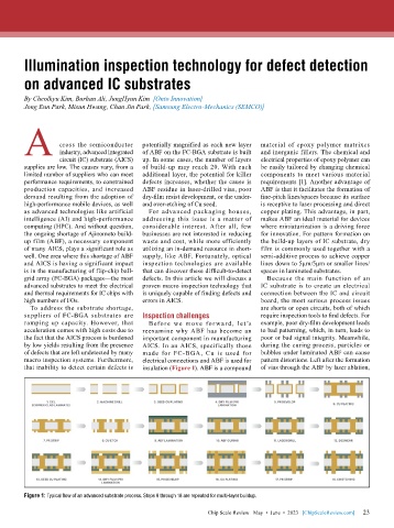
        that inability to detect certain defects is   insulation (Figure 1). ABF is a compound   of vias through the ABF by laser ablation,


        Figure 1: Typical flow of an advanced substrate process. Steps 9 through 18 are repeated for multi-layer buildup.

                                                                                                             23
                                                               Chip Scale Review   May  •  June  •  2023   [ChipScaleReview.com]  23

