Page 26 - Chip Scale Review_May June_2023-digital
P. 26
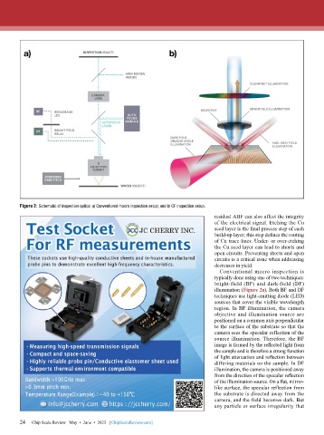
Figure 2: Schematic of inspection optics: a) Conventional macro inspection setup; and b) CF inspection setup.
                                                                              residual ABF can also affect the integrity
                                                                              of the electrical signal. Etching the Cu
                                                                              seed layer is the final process step of each
                                                                              build-up layer; this step defines the routing
                                                                              of Cu trace lines. Under- or over-etching
                                                                              the Cu seed layer can lead to shorts and
                                                                              open circuits. Preventing shorts and open
                                                                              circuits is a critical issue when addressing
                                                                              decreases in yield.
                                                                                Conventional  macro  inspection  is
                                                                              typically done using one of two techniques:
                                                                              bright-field (BF) and dark-field (DF)
                                                                              illumination (Figure 2a). Both BF and DF
                                                                              techniques use light-emitting diode (LED)
                                                                              sources that cover the visible wavelength
                                                                              region. In BF illumination, the camera
                                                                              objective and illumination source are
                                                                              positioned on a common axis perpendicular
                                                                              to the surface of the substrate so that the
                                                                              camera sees the specular reflection of the
                                                                              source illumination. Therefore, the BF
                                                                              image is formed by the reflected light from
                                                                              the sample and is therefore a strong function
                                                                              of light attenuation and reflection between
                                                                              differing materials on the sample. In DF
                                                                              illumination, the camera is positioned away
                                                                              from the direction of the specular reflection
                                                                              of the illumination source. On a flat, mirror-
                                                                              like surface, the specular reflection from
                                                                              the substrate is directed away from the
                                                                              camera, and the field becomes dark. But
                                                                              any particle or surface irregularity that


        24   Chip Scale Review   May  •  June  •  2023   [ChipScaleReview.com]
        24

