Page 27 - Chip Scale Review_May June_2023-digital
P. 27
scatters light out of the specular beam will   Imaging is accomplished using
        make the field bright. This characteristic   a high-resolution line scan
        makes DF illumination particularly good at   camera. The image pixel size
        identifying small particles and defects on a   corresponds to 0.7μm at 10X,
        flat specular surface.             which provides the highest
          We also used another inspection   level of magnification for
                                        ®
        illumination technology, Clearfind    inspection.
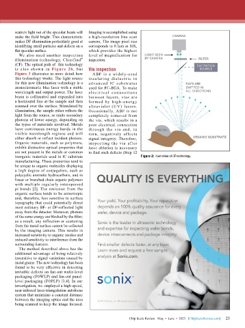
        (CF). The optical path of  this technology
        is also show n i n  Figure 2b, but    Via inspection
        Figure 3 illustrates in more detail how   ABF  is  a  widely-used
        this technology works. The light source   insulating dielect r ic in
        for this new illumination technology is a   advanced  IC  subst rates
        monochromatic blue laser with a stable   used for FC-BGA. To make
        wavelength and output power. The laser   ele c t r ic a l  c o n n e c t io n s
        beam is collimated and expanded into   between  layers,  vias  are
        a horizontal line at the sample and then   for med by h ig h- energ y
        scanned over the surface. Stimulated by   ultraviolet  (UV)  lasers.
        illumination, the sample either reflects the   Occasionally, ABF is not
        light from the source, or emits secondary   completely  removed  from
        photons of lower energy, depending on   the via, which results in a
        the types of materials involved. Metals   poor electrical connection
        have continuous energy bands in the   th rough  the  via  and,  in
        visible  wavelength  regions  and  will   t ur n,  negatively  affects
        either absorb or reflect incident photons.   signal integrity. Therefore,
        Organic materials, such as polymers,   inspecting  the  via  after
        exhibit distinctive optical properties that   laser ablation is necessary
        are not present in the metals or common   to find such defects (Step 12
        inorganic materials used in IC substrate                    Figure 3: Illustration of CF technology.
        manufacturing. These properties tend to
        be unique to organic molecules displaying
        a high degree of conjugation, such as
        polycyclic aromatic hydrocarbons, and in
        linear or branched chain organic polymers
        with multiple regularly interspersed
        pi bonds [2]. The emission from the
        organic surface tends to be anisotropic
        and, therefore, less sensitive to surface
        topography that could potentially direct
        most ordinary BF- or DF-reflected light
        away from the detector. Moreover, photons
        of the same energy are blocked by the filter;
        as a result, any reflection or scattering
        from the metal surface cannot be collected
        by the imaging camera. This results in
        increased sensitivity to organic residue and
        reduced sensitivity to interference from the
        surrounding features.
          The method described above has the
        additional advantage of being relatively
        insensitive to signal variations caused by
        metal grains. The new technology has been
        found to be very effective in detecting
        invisible defects on fan-out wafer-level
        packaging (FOWLP) and fan-out panel-
        level packaging (FOPLP) [3,4]. In our
        investigation, we employed a high-speed,
        near-infrared laser-triangulation autofocus
        system that maintains a constant distance
        between the imaging optics and the area
        being scanned to keep the image focused.


                                                                                                             25
                                                               Chip Scale Review   May  •  June  •  2023   [ChipScaleReview.com]  25

