Page 28 - Chip Scale Review_May June_2023-digital
P. 28
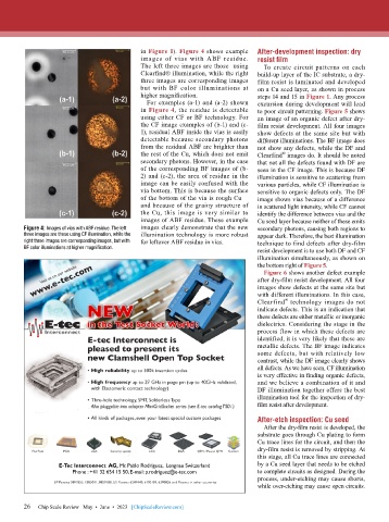
in Figure 1). Figure 4 shows example   After-development inspection: dry
                                           images  of  vias  with  ABF  residue.   resist film
                                           The left three images are those  using   To create circuit patterns on each
                                           Clearfind® illumination, while the right   build-up layer of the IC substrate, a dry-
                                           three images are corresponding images   film resist is laminated and developed
                                           but with BF color illuminations at   on a Cu seed layer, as shown in process
                                           higher magnification.              steps 14 and 15 in Figure 1. Any process
                                             For examples (a-1) and (a-2) shown   excursion during development will lead
                                           in Figure 4, the residue is detectable   to poor circuit patterning. Figure 5 shows
                                           using either CF or BF technology. For   an image of an organic defect after dry-
                                           the CF image examples of (b-1) and (c-  film resist development. All four images
                                           1), residual ABF inside the vias is easily   show defects at the same site but with
                                           detectable because secondary photons   different illuminations. The BF image does
                                           from the residual ABF are brighter than   not show any defects, while the DF and
                                           the rest of the Cu, which does not emit   Clearfind  images do. It should be noted
                                                                                      ®
                                           secondary photons. However, in the case   that not all the defects found with DF are
                                           of the corresponding BF images of (b-  seen in the CF image. This is because DF
                                           2) and (c-2), the area of residue in the   illumination is sensitive to scattering from
                                           image can be easily confused with the   various particles, while CF illumination is
                                           via bottom. This is because the surface   sensitive to organic defects only. The DF
                                           of the bottom of the via is rough Cu—  image shows vias because of a difference
                                           and because of the grainy structure of   in scattered light intensity, while CF cannot
                                           the Cu, this image is very similar to   identify the difference between vias and the
                                           images of ABF residue. These example   Cu seed layer because neither of these emits
        Figure 4: Images of vias with ABF residue. The left   images clearly demonstrate that the new   secondary photons, causing both regions to
        three images are those using CF illumination, while the   illumination technology is more robust   appear dark. Therefore, the best illumination
        right three images are corresponding images, but with   for leftover ABF residue in vias.  technique to find defects after dry-film
        BF color illuminations at higher magnification.                       resist development is to use both DF and CF
                                                                              illumination simultaneously, as shown on
                                                                              the bottom right of Figure 5.
                                                                                Figure 6 shows another defect example
                                                                              after dry-film resist development. All four
                                                                              images show defects at the same site but
                                                                              with different illuminations. In this case,
                                                                              Clearfind  technology images do not
                                                                                       ®
                                                                              indicate defects. This is an indication that
                                                                              these defects are either metallic or inorganic
                                                                              dielectrics. Considering the stage in the
                                                                              process flow in which these defects are
                                                                              identified, it is very likely that these are
                                                                              metallic defects. The BF image indicates
                                                                              some defects, but with relatively low
                                                                              contrast, while the DF image clearly shows
                                                                              all defects. As we have seen, CF illumination
                                                                              is very effective in finding organic defects,
                                                                              and we believe a combination of it and
                                                                              DF illumination together offers the best
                                                                              illumination tool for the inspection of dry-
                                                                              film resist after development.

                                                                              After-etch inspection: Cu seed
                                                                                After the dry-film resist is developed, the
                                                                              substrate goes through Cu plating to form
                                                                              Cu trace lines for the circuit, and then the
                                                                              dry-film resist is removed by stripping. At
                                                                              this stage, all Cu trace lines are connected
                   E-Tec Interconnect  AG, Mr. Pablo Rodriguez,  Lengnau Switzerland  by a Cu seed layer that needs to be etched
                       Phone : +41 32 654 15 50, E-mail: p.rodriguez@e-tec.com  to complete circuits as designed. During the
                                                                              process, under-etching may cause shorts,
                                                                              while over-etching may cause open circuits.


        26   Chip Scale Review   May  •  June  •  2023   [ChipScaleReview.com]
        26

