Page 29 - Chip Scale Review_May June_2023-digital
P. 29

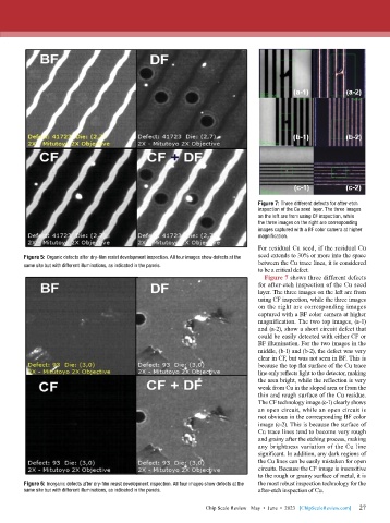
Figure 7: Three different defects for after-etch
                                                                              inspection of the Cu seed layer. The three images
                                                                              on the left are from using CF inspection, while
                                                                              the three images on the right are corresponding
                                                                              images captured with a BF color camera at higher
                                                                              magnification.
                                                                              For residual Cu seed, if the residual Cu
        Figure 5: Organic defects after dry-film resist development inspection. All four images show defects at the   seed extends to 30% or more into the space
        same site but with different illuminations, as indicated in the panels.  between the Cu trace lines, it is considered
                                                                              to be a critical defect.
                                                                                Figure 7 shows three different defects
                                                                              for after-etch inspection of the Cu seed
                                                                              layer. The three images on the left are from
                                                                              using CF inspection, while the three images
                                                                              on the right are corresponding images
                                                                              captured with a BF color camera at higher
                                                                              magnification. The two top images, (a-1)
                                                                              and (a-2), show a short circuit defect that
                                                                              could be easily detected with either CF or
                                                                              BF illumination. For the two images in the
                                                                              middle, (b-1) and (b-2), the defect was very
                                                                              clear in CF, but was not seen in BF. This is
                                                                              because the top flat surface of the Cu trace
                                                                              line only reflects light to the detector, making
                                                                              the area bright, while the reflection is very
                                                                              weak from Cu in the sloped area or from the
                                                                              thin and rough surface of the Cu residue.
                                                                              The CF technology image (c-1) clearly shows
                                                                              an open circuit, while an open circuit is
                                                                              not obvious in the corresponding BF color
                                                                              image (c-2). This is because the surface of
                                                                              Cu trace lines tend to become very rough
                                                                              and grainy after the etching process, making
                                                                              any brightness variation of the Cu line
                                                                              significant. In addition, any dark regions of
                                                                              the Cu lines can be easily mistaken for open
                                                                              circuits. Because the CF image is insensitive
                                                                              to the rough or grainy surface of metal, it is
        Figure 6: Inorganic defects after dry-film resist development inspection. All four images show defects at the   the most robust inspection technology for the
        same site but with different illuminations, as indicated in the panels.  after-etch inspection of Cu.

                                                                                                             27
                                                               Chip Scale Review   May  •  June  •  2023   [ChipScaleReview.com]  27
   24   25   26   27   28   29   30   31   32   33   34