Page 37 - Chip Scale Review_January February_2023-digital
P. 37
Oxide crack risk assessment during probing over


        active area

        By Oliver Nagler, Marianne Unterreitmeier  [Infineon Technologies AG]

        C         o n t i n u ou s l y  s m a l l e r


                  structural sizes of integrated
                  circuits (ICs) of advanced
        semiconductors, higher signal integrity,
        faster switching speed, new materials,
        a nd  desig n  opt i m i zat ions,  br i ng
        essential performance benefits and yield
        improvements to electronic devices. On
        the other hand, during wafer test, it is
        getting more and more important to use
        the complete surface of the wafer for
        probing and bonding instead of placing
        contact pads outside the active circuit
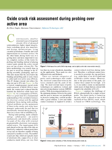
        area on top of pure silicon (Si). The   Figure 1: POAA layout for a) (left) CMOS chip design, and b) (right) a schematic cross-section view [2].
        latter methodology was usually done in
        the past to avoid any damage to the IC   less than ten, to up to hundreds, depending   contact-related yield loss during wafer
        during assembly, packaging, and test.   on the application. These pads are also   test. Therefore, a sufficient contact force
        This also means that the area below the   different in size and thickness.  is needed to penetrate the top pad layer
        bonding and probing pads is used, which   There are various categories of   (e.g., oxide layer of an Al-Cu pad) and
        is called pad-over-active-area (POAA).   probe card technologies that enable   establish a stable contact. However,
        This IC design concept can reduce the   the electrical connection between the   due to the placement of the pads, the
        chip size up to 20% (see Figure 1a). For   tester channels and the pads of the   contact force cannot be too high—if it
        a typical complementary metal-oxide   chip. The most-relevant types of probe   is, it can induce cracks in intermediate
        semiconductor (CMOS) POAA layer    technologies are cantilever, vertical, and   oxide layers of chips that are critical with
        stack, the contact pad is placed directly   microelectromechanical system (MEMS)   regard to the reliability of ICs [3].
        beneath the dielectric oxide layer (see   probes. With decreasing pad pitches (i.e.,   Figure 2 explains the challenge of
        Figure 1b). As a consequence of POAA,   the minimum distance between two pads)   POAA schematically for a single vertical
        there is a great need for a fundamental   and the goal to increase test parallelism   probe. The elastic probe is contacting
        understanding of the correlation between   to decrease testing time, vertical needles   the pad, which is placed on top of the
        the electrical contact and the applied   offer a good solution. A low and stable   backend-of-line (BEOL) stack, which
        mechanical forces during wafer probing.   contact resistance is required to avoid a   is based on CMOS technology. The
        Typical problems are the appearance
        of deep probe marks and oxide layer
        damages underneath the pad that are
        mechanically stressed during probing—
        these are a severe risk to reliability [1,2].
          During wafer probing, elastic contactor
        springs – called probes – are used to
        mechanically and electrically connect
        the pads of the chip with external
        programmable electronic instruments
        called testers. The input/output (I/O)
        pads placed on the top side of the chip are
        electrically conductive without passivation
        on top and are therefore capable of being
        contacted by needles or wires. The number
        of pads per chip, which are typically made
        of aluminum (Al), copper (Cu), or other
        conductive metal alloys, can vary from   Figure 2: Vertical probe contacting a POAA, thereby inducing oxide cracks [2].


                                                                                                             35
                                                          Chip Scale Review   January  •  February  •  2023   [ChipScaleReview.com]  35

