Page 39 - Chip Scale Review_January February_2023-digital
P. 39
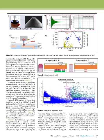
Figure 5: a) Patented sensor-indenter system; b) Crack detection by AE test method; c) Acoustic signal in time and frequency domains; and d) Typical contact cycle.
        determine the crack probability during wafer
        probing under conditions that occur during
        manufacturing, and to identify the most
        robust pad stack design in order to avoid
        oxide cracks. The first chip variant (option A)
        has a Cu-pad on top with a “checkerboard”
        routing pattern in the upper oxide layer and
        another metal fill in the oxide layer below.
        In contrast, the second variant (option B)   Figure 6: Pad stack options A and B.
        has the same pad metal design, but a double
        oxide layer without metal routing in the
        upper-most isolation layers (Figure 6).
          In order to assess the risk of generating
        probing-related cracks, the tolerances of
        the probe geometries are considered during
        the study. Two different tip diameters, 5µm
        and 10µm, were used for the contact cycles.
        The tips are flat with a small edge radius
        representing the typical dimensions and
        geometry of a manufacturing probe card for
        a similar range of contact force.
          In total, 150 contact cycles with a
        maximum contact force of 250mN for each
        pad stack/tip combination were performed
        to achieve nearly 100% crack probability.
        During contacting, the AE signals were
        cumulatively recorded and later graphically   Figure 7: Scatter plot of clustered AE signals.
        visualized in a scatter plot (Figure 7).
        The burst signal energy in units of eu   decreasing during penetration of the pad   inspections.  For  a  meaningful  data
              14
                2
        (1eu=10 V s) is used here as a characteristic   metal up to a critical contact force of around   clustering of those hits, when “first
        feature of an AE event.            100mN—meaning no AE crack events were   oxide cracks” appear, it is important to
          Figure 7 shows the burst signal energy   observed. For a contact force higher than   correctly set the filter limits of contact
        in logarithmic scale as a function of contact   100mN, the burst signal energy of the hits is   force and burst energy. Therefore, only
        force for all hits derived during 150 contact   increasing again.     hits with energy higher than 5eu of each
        cycles for pad option A and a tip diameter of   In the case of a crack, the burst signal   contact cycle, occurring at a certain
        5µm. Here, one can see that the burst signal   energy is assumed to be higher than   contact force, are included and utilized
        energies are high at the beginning and   5eu, which was correlated by optical   for further data clustering. Hits with a


                                                                                                             37
                                                          Chip Scale Review   January  •  February  •  2023   [ChipScaleReview.com]  37

