Page 41 - Chip Scale Review_January February_2023-digital
P. 41
and other stress-related processes during
                                                                              the manufacturing flow.

                                                                              Acknowledgment
                                                                                Portions of this article were presented
                                                                              at SWTest 2022.
                                                                              References
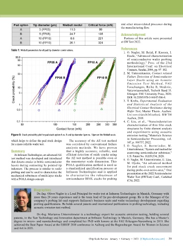
        Table 1: Weibull parameters for all pad/tip diameter combinations.
                                                                                1.  O. Nagler, M. Reinl, F. Kaesen, I.
                                                                                  Eisele, “Advanced characterization
                                                                                  of semiconductor wafer probing
                                                                                  methodology,” Proc. of the 23rd
                                                                                  International Conf. on Electrical
                                                                                  Contacts, Sendai, 2006, pp. 97–102.
                                                                                2.  M. Unterreitmeier, Contact related
                                                                                  Failure Detection of Semiconductor
                                                                                  Layer Stacks using an Acoustic
                                                                                  E mi s sio n Te st Me th o d,  FAU
                                                                                  Forschungen, Reihe B, Medizin,
                                                                                  Naturwissenschaft, Technik Band 33.
                                                                                  Erlangen: FAU University Press, 2020.
                                                                                  DOI: 10.25593/978-3-96147-306-9.
                                                                                3.  T. Krebs, Experimental Evaluation
                                                                                  and Statistical Analysis of the
                                                                                  Electrical Contact Resistance during
                                                                                  Wafer Test; Master Thesis. Aachen:
                                                                                  Universitätsbibliothek  RWTH
                                                                                  Aachen, 2018.
                                                                                4.  C. Liu, et al., “Nanoindentation
                                                                                  characterization of thin film stack
                                                                                  structures by finite element analysis
                                                                                  and  experiments  using  acoustic
        Figure 9: Crack probability plot for pad stack option A vs. B and tip diameter 5µm vs. 10µm on the Weibull scale.  emission testing,”Materials Science
                                                                                  in Semiconductor Processing, vol.
        which helps to define the pad stack design   The accuracy of the AE test method   147, p. 106737, 2022.
        for a more reliable wafer test.    was correlated by conventional failure   5.  O. Nagler, S. Ber n rieder, M.
                                           analysis  methods.  We  have  proven   Unterreitmeier, “System and method for
        Summary                            that a highly accurate, reliable, and   examining semiconductor substrates,”
          At Infineon Technologies, an advanced AE   efficient detection of oxide cracks using   U.S. Patent No. 10,859,534, 2020.
        test method was developed and introduced   the AE test method is possible even at   6.  O. Nagler, M. Unterreitmeier, E. Liau,
        that detects cracks in brittle semiconductor   the nanometer scale dimension. This   M. Ojeda, “An advanced method
        layers during contacting by pointed tip   POAA qualification method is used as   for  pad  stack  crack  assessment
        indenters. The process is similar to wafer   a standardized qualification process at   during probe-over-active-area,” Oral
        probing and can be used to characterize the   Infineon Technologies and is applied   presentation at the 2022 Semiconductor
        mechanical robustness of multi-layer stacks   to characterize the robustness of   Wafer Test (SWTest) Conf., Carlsbad
        with a POAA design concept.        semiconductor BEOL stacks for probing   (CA), 2022.


                       Biographies
                         Dr.-Ing. Oliver Nagler is a Lead Principal for wafer test at Infineon Technologies in Munich, Germany with
                       more than 20 years experience and is the team lead of the pre-development group. He is the Manager of the
                       company’s probing lab and supports Infineon’s business units and wafer technology development regarding
                       probing qualifications. He holds several patents and international publications in probing technology, including
                       acoustic emission test method.
                         Dr.-Ing. Marianne Unterreitmeier is a technology expert for acoustic emission testing, holding several
          patents, in the Test Technology and Innovation department at Infineon Technology in Munich, Germany. She has a Master’s
          degree in micro- and nanotechnology and completed her PhD with honors at the FAU Erlangen-Nuremberg in 2019. She
          achieved the Best Paper Award at the ESREF 2018 conference in Aalborg and the Regensburger Award for Women in Science
          and Art in 2021.


                                                                                                             39
                                                          Chip Scale Review   January  •  February  •  2023   [ChipScaleReview.com]  39

