Page 38 - Chip Scale Review_January February_2023-digital
P. 38
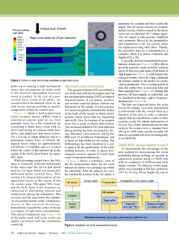
penetrates the couplant and then reaches the
                                                                              sensor. The AE sensor converts the dynamic
                                                                              surface-motion, which is caused by the elastic
                                                                              wave, into an electrical (AC) voltage signal.
                                                                              The AE signal is subsequently amplified
                                                                              and commonly filtered by the preamplifier
                                                                              and transmitted to the AE system where
                                                                              the signal processing takes place. Finally,
                                                                              the generated data set is transmitted to a
                                                                              computer where it is stored, evaluated, and
                                                                              displayed [2; p. 81].
                                                                                A specially developed and patented sensor-
                                                                              indenter system (see Figure 5a) [4] is able to
                                                                              precisely generate cracks in brittle isolation
                                                                              layers of thin-layer pad stacks of all kinds of
                                                                              chip designs (see Figure 5b) and measure the
                                                                              released acoustic waves by using a diamond
        Figure 3: Stress in a layer stack during contacting causing oxide cracks.  tip indenter similar to the probes of a probe
                                                                              card in production. Over a certain period of
        probe tip is causing a high mechanical   Pad stack crack assessment   time, the contact force is increased, held, and
        stress that can generate an oxide crack   The acoustic emission (AE) test method is   then unloaded (see Figure 5d). During this
        if  the  material-dependent  fractural   one of the most efficient techniques used for   process, AE burst signals, so-called hits, can
        stress is reached. In the case of a pure   the non-destructive testing (NDT) of material   be visualized in the time- and/or frequency-
        vertical force vector of the probe, the   characterization. It can detect, localize,   domains (see Figure 5c).
        contact-related mechanical stress in the   and monitor material defects without any   The hits are triggered above the noise
        thin layers during probing is mostly   destruction of the sample. For this purpose,   threshold voltage, recorded, and plotted
        compressive within the contact area.  AE sensors are glued or pressed to the surface   synchronized with the contact force as a
          Figure 3a shows a half-symmetrical   of the body of the sample to detect elastic   function of the time in order to identify
        finite-element  model  (FEM)  with  a   acoustic shock waves that are expanding   signals that are classified as cracks or other
        simulated  contour  plot  of  the  first   spherically from the location of an acoustic   acoustic events like plastic deformation or
        principle stress for a flat cylindrical tip   event like a crack or plastic deformation.   friction. For a better statistically-proven data
        contacting a multi-layer stack with an   This advanced method of AE crack detection   analysis, the contact cycle is repeated from
        Al-Cu pad on top of a silicon oxide layer   during probing has been developed by Dr.-  100 up to 1,000 times and the recorded AE
        (SiO 2 ) and additional thin layers below.   Ing. Marianne Unterreitmeier during her   data are cumulated and saved chronologically
        For a flat tip of 10µm diameter and at a   PhD work [2] at Infineon Technologies, and   in an ASCII file.
        maximum contact force of 300mN, the   is based on state-of-the-art AE testing. The
        highest stress values are approximately   methodology has been modified in a way
        ±8.02N/m² (=8.02GPa) and are located   to apply it for the qualification of the wafer   CMOS BEOL design options A and B
        below the center of the indenter tip in the   probing process, in order to detect low-  To demonstrate the advantage of the
        region of the Si 3 N 4  layer below the upper   energetic acoustic signals of brittle layer   new method for determining the crack
        SiO 2  layer.                      cracks in nanometer dimensions.    probability during probing, we present an
          With increasing contact force, the SiO 2    Figure 4 shows a schematic view of   application example using a CMOS chip
        layer is elastically deflected downwards   the AE measurement chain. An AE event   with an evaluation of different pad stack
        at the same time the Al-Cu pad metal   releases an elastic wave propagating within   design variants. The objective of this study,
        and the Cu layer below are plastically   the solid body. After the induced AE wave   which was presented at SWTest conference
        deformed  under  vertical  load.  This   has reached the location of the AE sensor, it   2022 by Dr.-Ing. Oliver Nagler [5], was to
        creates a U-shaped deformation of the
        uppermost layers in the region of the
        tip contact area. The upper SiO 2  layer
        and the Si 3 N 4  layer of the structure are
        subjected to alternating tension and
        compression during the indentation. The
        Cu layer and the area below the indenter
        tip are predominantly under compressive
        st ress i n t he ve r t ical d i re ct ion.
        Immediately beneath the center of the tip
        is a region of high stress concentration.
        The optical inspections (see Figure 3b)
        of the probe mark and oxide cracks are
        highly correlated with the simulation
        results [4].                       Figure 4: Schematic view of AE measurement chain [2].

        36
        36   Chip Scale Review   January  •  February  •  2023   [ChipScaleReview.com]

