Page 32 - Chip Scale Review_January February_2023-digital
P. 32
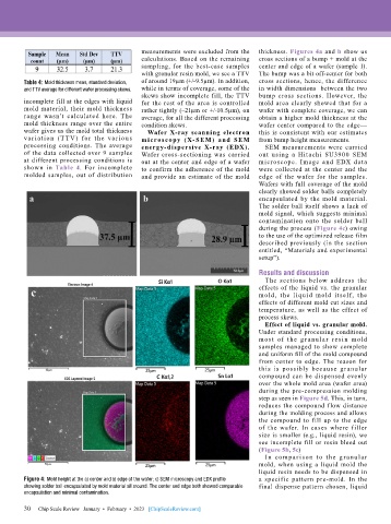
measurements were excluded from the   thickness. Figures 4a and b show us
                                           calculations. Based on the remaining   cross sections of a bump + mold at the
                                           sampling,  for  the  best-case  samples   center and edge of a wafer (sample 1).
                                           with granular resin mold, we see a TTV   The bump was a bit off-center for both
        Table 4: Mold thickness mean, standard deviation,   of around 19µm (+/-9.5µm). In addition,   cross sections, hence, the difference
        and TTV average for different wafer processing skews.  while in terms of coverage, some of the   in width dimensions  between the two
                                           skews show incomplete fill, the TTV   bump  cross  sections.  However,  the
        incomplete fill at the edges with liquid   for the rest of the area is controlled   mold  area  clearly  showed  that  for  a
        mold  material,  their  mold  thickness   rather tightly (~21µm or +/-10.5µm), on   wafer with complete coverage, we can
        range wasn’t calculated here. The   average, for all the different processing   obtain a higher mold thickness at the
        mold thickness range over the entire   condition skews.               wafer center compared to the edge—
        wafer gives us the mold total thickness   Wafer X-ray scanning electron   this is consistent with our estimates
        va r iat ion  (T T V )  for t he  va r ious   m icroscopy ( X- SEM ) and SEM   from bump height measurements.
        processing conditions. The average   energy-dispersive X-ray (EDX).     SEM  measurements  were  carried
        of the data collected over 9 samples   Wafer cross-sectioning was carried   out  using  a  Hitachi  SU3900  SEM
        at different processing conditions is   out at the center and edge of a wafer   microscope.  Image  and  EDX  data
        shown in  Table 4.  For  incomplete   to confirm the adherence of the mold   were collected at the center and the
        molded  samples,  out  of  distribution   and provide an estimate of the mold   edge  of  the  wafer  for  the  samples.
                                                                              Wafers with full coverage of the mold
                                                                              clearly showed solder balls completely
                                                                              encapsulated  by  the  mold  material.
                                                                              The solder ball itself shows a lack of
                                                                              mold signal, which suggests minimal
                                                                              contamination  onto  the  solder  ball
                                                                              during the process (Figure 4c) owing
                                                                              to the use of the optimized release film
                                                                              described previously (in the section
                                                                              entitled, “Materials and experimental
                                                                              setup”).

                                                                              Results and discussion
                                                                                The sections below address the
                                                                              effects of the liquid vs. the granular
                                                                              mold,  the  liquid  mold  itself,  the
                                                                              effects of different mold cut sizes and
                                                                              temperature, as well as the effect of
                                                                              process skews.
                                                                                Effect of liquid vs. granular mold.
                                                                              Under standard processing conditions,
                                                                              most  of  the  g ranula r  resi n  mold
                                                                              samples  managed  to  show  complete
                                                                              and uniform fill of the mold compound
                                                                              from center to edge. The reason for
                                                                              this is possibly because granular
                                                                              compound  can  be  dispensed  evenly
                                                                              over the whole mold area (wafer area)
                                                                              during the pre-compression molding
                                                                              step as seen in Figure 5d. This, in turn,
                                                                              reduces the compound flow distance
                                                                              during the molding process and allows
                                                                              the compound to fill up to the edge
                                                                              of the wafer. In cases where filler
                                                                              size is smaller (e.g., liquid resin), we
                                                                              see incomplete fill or resin bleed out
                                                                              (Figure 5b, 5c)
                                                                                I n  compa r ison  to  the  g ranula r
                                                                              mold,  when  using  a  liquid  mold  the
                                                                              liquid resin needs to be dispensed in
        Figure 4: Mold height at the a) center and b) edge of the wafer; c) SEM microscopy and EDX profile   a  specific  pattern  pre-mold.  In  the
        showing solder ball encapsulated by mold material all around. The center and edge both showed comparable   final dispense pattern chosen, liquid
        encapsulation and minimal contamination.

        30
        30   Chip Scale Review   January  •  February  •  2023   [ChipScaleReview.com]

