Page 29 - Chip Scale Review_January February_2023-digital
P. 29
The target products were 12-inch
                                                                              silicon wafers (~775µm) + Cu Pillar +
                                                                              SnAg µBump (~45µm). Shallow edge
                                                                              trim was used on these wafers to clean
                                                                              the wafer edge and allow for better
                                                                              clamping of the wafers during the mold
                                                                              process and prevent any leakage of
                                                                              resin material. Consequently, the thin
                                                                              resin  layer  of  30μm  is  molded  onto
                                                                              the wafers, while leaving the top of
                                                                              the solder ball exposed over the entire
                                                                              wafer (Figure 1b).
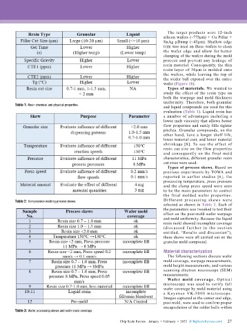
                                                                                Types of materials. We wanted to
                                                                              study the effect of the resin type on
                                                                              both the warpage and mold thickness
                                                                              uniformity. Therefore, both granular
        Table 1: Resin chemical and physical properties.                      and liquid compounds are used for this
                                                                              evaluation (Table 1). Liquid resin has
                                                                              a number of advantages including a
                                                                              lower melt viscosity that allows better
                                                                              flow properties and easily fills tighter
                                                                              pitches. Granular compounds, on the
                                                                              other hand, have a longer shelf life,
                                                                              lower material cost, and lower material
                                                                              shrinkage [8]. To see the effect of
                                                                              resin cut size on the flow properties
                                                                              and  consequently  on  the  final  mold
                                                                              characteristics, different granular resin
                                                                              cut sizes were used.
                                                                                Types of process skews. Based on
                                                                              previous experiments by TOWA and
                                                                              reported in earlier studies [6], the
                                                                              processing temperature, press pressure
                                                                              and the clamp press speed were seen
                                                                              to be the main parameters to control
                                                                              the  final  molded  wafer  properties.
        Table 2: Compression molding process skews.                           Different processing skews were
                                                                              selected as shown in Table 2. Each of
                                                                              the parameters was tweaked to test their
                                                                              effect on the post-mold wafer warpage
                                                                              and mold uniformity. Because the liquid
                                                                              resin mold showed incomplete coverage
                                                                              (discussed f ur ther in the section
                                                                              entitled,  “Results  and  discussion”),
                                                                              these skews were all carried out on the
                                                                              granular mold compound.
                                                                              Material characterization
                                                                                The following sections discuss wafer
                                                                              mold coverage, warpage measurements,
                                                                              mold height measurements, and various
                                                                              scanning electron microscope (SEM)
                                                                              measurements.
                                                                                Wafer mold  coverage.  Optical
                                                                              microscopy  was  used  to  verify  full
                                                                              wafer coverage by mold material using
                                                                              a  Keyence  V K-3000  microscope.
                                                                              Images captured at the center and edge,
                                                                              post mold, were used to confirm proper
                                                                              encapsulation of the solder balls within
        Table 3: Wafer processing skews and wafer mold coverage.

                                                                                                             27
                                                          Chip Scale Review   January  •  February  •  2023   [ChipScaleReview.com]  27

