Page 31 - Chip Scale Review_January February_2023-digital
P. 31
the mold material and therefore, the full
                                                                              coverage of the wafer. All the different
                                                                              process skews and their mold coverage
                                                                              were tabulated (Table 3). Results
                                                                              were further discussed in the section
                                                                              entitled, “Results and discussion.”
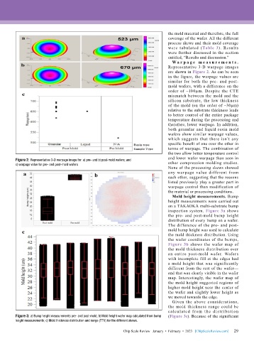
                                                                                W a r p a g e me a s u r e me n t s .
                                                                              Representative 3-D warpage images
                                                                              are shown in Figure 2. As can be seen
                                                                              in the figure, the warpage values are
                                                                              similar  for  both  the  pre-  and  post-
                                                                              mold wafers, with a difference on the
                                                                              order  of  ~100µm.  Despite  the  CTE
                                                                              mismatch between the mold and the
                                                                              silicon substrate, the low thickness
                                                                              of the mold (on the order of ~30µm)
                                                                              relative to the substrate thickness leads
                                                                              to better control of the entire package
                                                                              temperature during the processing and
                                                                              therefore, lower warpage. In addition,
                                                                              both granular and liquid resin mold
                                                                              wafers show similar warpage values,
                                                                              which suggests that there isn’t any
                                                                              specific benefit of one over the other in
                                                                              terms of warpage. The combination of
                                                                              the two allow better temperature control
                                                                              and lower wafer warpage than seen in
        Figure 2: Representative 3-D warpage image for: a) pre- and b) post-mold wafers; and
        c) warpage value for pre- and post-mold wafers                        other  compression  molding  studies.
                                                                              None of the processing skews showed
                                                                              any  warpage  value  different  from
                                                                              each other, suggesting that the reasons
                                                                              listed previously play a greater part in
                                                                              warpage control than modification of
                                                                              the material or processing conditions.
                                                                                Mold height measurements. Bump
                                                                              height measurements were carried out
                                                                              on a TAKAOKA multi-substrate bump
                                                                              inspection system. Figure 3a shows
                                                                              the pre- and post-mold bump height
                                                                              distribution of every bump on a wafer.
                                                                              The difference of the pre- and post-
                                                                              mold bump height was used to calculate
                                                                              the mold thickness distribution. Using
                                                                              the wafer coordinates of the bumps,
                                                                              Figure 3b  shows  the  wafer  map  of
                                                                              the mold thickness distribution over
                                                                              an  entire  post-mold  wafer.  Wafers
                                                                              with incomplete fill at the edges had
                                                                              a mold height that was significantly
                                                                              different from the rest of the wafer—
                                                                              and that was clearly visible in the wafer
                                                                              map. Interestingly, the wafer map of
                                                                              the mold height suggested regions of
                                                                              higher mold height near the center of
                                                                              the wafer and slightly lower height as
                                                                              we moved towards the edge.
                                                                                Given the above considerations,
                                                                              the  mold  thickness  range  could  be
                                                                              calculated  f rom  the  dist r ibution
        Figure 3: a) Bump height measurements pre- and post-mold; b) Mold height wafer map calculated from bump   (Figure 3c). Because of the significant
        height measurements; c) Mold thickness distribution and range (TTV) for the different skews.

                                                                                                             29
                                                          Chip Scale Review   January  •  February  •  2023   [ChipScaleReview.com]  29

