Page 26 - Chip Scale Review_January February_2023-digital
P. 26
•  Repeating defects, which suggest
                                                                                  mask or reticle errors; and
                                                                                •  Variable bump height distribution,
                                                                                  which  can  reveal  performance
                                                                                  d if fe re nce s bet we e n plat i ng
                                                                                  machines or plating cells.
                                                                                The results of these measurements
                                                                              allow operators to adjust the process
                                                                              in  real  time  to  improve  yield  and
                                                                              reduce the need for rework. Why
                                                                              wouldn’t a fab do 100% inspection?
                                                                              The answer lies in the method. Probe
                                                                              cards,  for  example,  can  measure  an
                                                                              entire wafer at once but cause damage
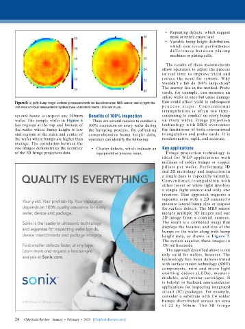
        Figure 6: a) (left) Bump height uniformity measured with the NanoResolution MRS sensor, and b) (right) the   that could affect yield in subsequent
        reference confocal measurement system show consistent results. Units are in µm.  p r o c e ss  s t e ps .  Co n v e n t i o n al
                                                                              t r ia ng u lat ion  is  of ten  too  t i me -
        several hours to inspect one 300mm   Benefits of 100% inspection      consuming to conduct on every bump
        wafer. The sample wafer in Figure 6   There are several reasons to conduct a   on  every  wafer.  Fringe  projection
        has regions at the top and bottom of   100% inspection on every wafer during   technology  with  MRS  overcomes
        the wafer where bump height is low   the  bumping  process.  By  collecting   the limitations of both conventional
        and regions at the sides and center of   comprehensive  bump  height  data,   triangulation and probe cards. It is
        the wafer where bumps are higher than   operators can identify the following:  nondestructive, rapid, and accurate.
        average. The correlation between the
        two images demonstrates the accuracy   •  Cluster defects, which indicate an   Key applications
        of the 3D fringe projection data.      equipment or process issue;      Fringe  projection  technology  is
                                                                              ideal  for  W LP  applications  with
                                                                              millions  of  solder  bumps  or  copper
                                                                              pillars  per  wafer.  Perfor ming  3D
                                                                              and 2D metrology and inspection in
                                                                              a single pass is especially valuable.
                                                                              Convent ional t r iang ulat ion with
                                                                              either lasers or white light involves
                                                                              a  single  light  source  and  only  one
                                                                              receiver.  That  approach  requires  a
                                                                              separate  scan  with  a  2D  camera  to
                                                                              measure lateral bump size or inspect
                                                                              for surface defects. The MRS sensor
                                                                              merges multiple 3D images and one
                                                                              2D  image  from  a  coaxial  camera.
                                                                              The result is a combined image that
                                                                              displays the location and size of the
                                                                              bumps on the wafer along with bump
                                                                              height data, as shown in  Figure 7.
                                                                              The system acquires these images in
                                                                              150 milliseconds.
                                                                                The approach described above is not
                                                                              only valid for wafers, however. The
                                                                              technology  has  been  demonstrated
                                                                              with surface mount technology (SMT)
                                                                              components,  mini  and  micro  light
                                                                              emitting  didoes  (LEDs),  memor y
                                                                              modules,  and  printer  cartridges.  It
                                                                              is helpful in backend semiconductor
                                                                              applications for inspecting integrated
                                                                              circuit  (IC)  packages.  For  example,
                                                                              consider a substrate with C4 solder
                                                                              bumps  distributed  across  an  area
                                                                              of  2 2  by  50 m m .  T h e  3D  f r i nge


        24   Chip Scale Review   January  •  February  •  2023   [ChipScaleReview.com]
        24

