Page 21 - Chip Scale Review_January February_2023-digital
P. 21
FOWLP adoption in mobile products.
                                                                              In addition to cost reduction for a given
                                                                              product, broadening its adoption or
                                                                              application to diverse systems would
                                                                              be good alternatives to managing the
                                                                              manufacturing cost. Fortunately, more
                                                                              opportunities with respect to advanced
                                                                              packaging technologies are open to
                                                                              many DRAM-related systems and the
                                                                              use of FOWLP in DRAM packaging is
                                                                              one of them.

                                                                              Acknowledgment
                                                                                This article in original content and
                                                                              format  was  presented  at  the  ECTC
                                                                              2022 Conference. It has been edited for
                                                                              publication in Chip Scale Review.

                                                                              References
                                                                                1.  H.  Y.  Son,  et  al.,  “Reliability
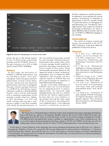
        Figure 13: Delta of the timing margin as a function of clock speed.
                                                                                  st ud ie s  on  m ic ro - bu mp s  for
        speed, the gap of the timing margin   the two different packages should   3-D  TSV  i nteg rat ion,”  Proc.
        is only 7% between the conventional   be well matched. Enhanced thermal   in  Electronic  Components  and
        package  and  the  FOWLP.  However,   performance that results when using   Technology Conference (ECTC)
        the gap increases up to 22% at high   a thinner package height would be a   (2013).
        speeds around 6000~6400Mbps.       potential advantage considering the   2.  H.  Y.  Son,  et  al.,  “Interconnect
                                           future trends of SoC power being       challenges in memory packaging,”
        Summary                            incrementally increased. Moreover, the   19th International Symposium on
          In this study, the utilization of   improved results in terms of electrical   Microelectronics and Packaging
        FOWLP  in  DRAM  applications  and   performance such as channel SI, PDN   (2021).
        the HIFOM str uct ure  have been   impedance,  and  crosstalk,  can  have   3.  Chien-Fu  Tseng,  et  al.,  “InFO
        introduced. These structures and their   superior aspects of FOWLP that can   (wafer level integrated fan-out)
        effectiveness in terms of form factor,   drive and accelerate its adoption to   technology,” Proc. ECTC (2016).
        thermal,  mechanical  and  electrical   both DRAM and AP packages.      4.  J. H. Lau, et al., “Reliability of
        performances, have been investigated.   In spite of the huge advantages of   fan-out wafer-level packaging
        Having a thinner package thickness   FOWLP,  there  are  several  hurdles   with  large  chips  and  multiple
        in a FOWLP by eliminating organic   for  its  implementation  to  mobile   redistributed layers,” Proc. ECTC
        substrates would be a distinguishable   applicat ion s.  As  expected ,  h ig h   (2018).
        benefit—and it will be well aligned   manufacturing cost can be a critical   5.  J. H. Kim et al., “Evaluation of
        with a consistent requirement on the   problem  for  mobile  applicat ions   chip stackable FOWLP technology
        package z-height reduction. Adding   because they are very sensitive to   for  high-performance  and  large
        to t h is adva nt age, low CT E a nd   the product cost and the value chain   memory capacity,” Proc. in Korean
        small  warpage  may  provide  a  wide   of  the  ecosystem  is  determined  by   Microelectronics and Packaging
        process window in the PoP assembly   cost competitiveness. Cost reduction   Society (2020).
        with  which  the  thermal  behavior  of   activit y is def initely needed for

                       Biographies
                         Ho-Young Son is a Principal Engineer and project leader of the integrated interconnect packaging development
                       team at SK hynix Inc., Icheon-si, Gyeonggi-do, Republic of Korea. He received a PhD in Materials Science and
                       Engineering from KAIST. Since he joined SK hynix in 2008, he has led the package development of world-
                       first HBM product and high-density memory modules by implementing a mass reflow bonding process. He
                       is currently leading advanced packaging technology related to 3D/TSV and FOWLP technology, not only for
                       leading-edge memory products, but also for future 2.5D/3D chiplet applications. Email hoyoung.son@sk.com

            Ki-Jun Sung is a Senior Engineer of the integrated interconnect packaging development team at SK hynix Inc., Icheon-si,
          Gyeonggi-do, Republic of Korea. He received his MS from the Department of Advanced Device Technology, U. of Science
          and Technology, Rep. of Korea. He joined SK hynix Inc. in 2011 and worked as a Process Engineer for memory embedded and
          2.5D packaging. His research activities include the development of the fabrication and interconnection for advanced packaging
          technology related to FOWLP technology.


                                                                                                             19
                                                          Chip Scale Review   January  •  February  •  2023   [ChipScaleReview.com]  19

