Page 18 - Chip Scale Review_January February_2023-digital
P. 18
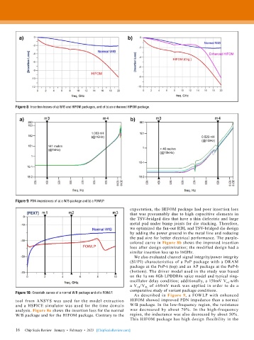
Figure 8: Insertion losses of a) W/B and HIFOM packages, and of b) an enhanced HIFOM package.


        Figure 9: PDN impedances of a) a W/B package and b) a FOWLP.
                                                             expectation, the HIFOM package had poor insertion loss
                                                             that was presumably due to high capacitive elements in
                                                             the TSV-bridged dies that have a thin dielectric and large
                                                             metal pad under bump joints for die stacking. Therefore,
                                                             we optimized the fan-out RDL and TSV-bridged die design
                                                             by adding the power ground in the metal line and reducing
                                                             the pad size for better electrical performance. The purple-
                                                             colored curve in Figure 8b shows the improved insertion
                                                             loss after design optimization; the modified design had a
                                                             similar insertion loss up to 16GHz.
                                                               We also evaluated channel signal integrity/power integrity
                                                             (SI/PI) characteristics of a PoP package with a DRAM
                                                             package at the PoP-t (top) and an AP package at the PoP-b
                                                             (bottom). The driver model used in the study was based
                                                             on the 1a nm 8Gb LPDDR4x spice model and typical ring-
                                                             oscillator delay condition; additionally, a 150mV V ref  with
                                                             a V IH /V IL   of  ±60mV  mask  was  applied  in  order  to  do  a
                                                             comparative study of variant package conditions.
        Figure 10: Crosstalk curves of a normal W/B package and of a FOWLP.
                                                               As described in  Figure 9,  a  FOWLP  with  enhanced
        tool  from  ANSYS  was  used  for  the  model  extraction   HIFOM showed improved PDN impedance than a normal
        and  a  HSPICE  simulator  was  used  for  the  time  domain   W/B package. In the low-frequency region, the resistance
        analysis. Figure 8a shows the insertion loss for the normal    was  decreased  by  about  70%.  In  the  high-frequency
        W/B package and for the HIFOM package. Contrary to the   region, the inductance was also decreased by about 50%.
                                                             This HIFOM package has high design flexibility in the

        16   Chip Scale Review   January  •  February  •  2023   [ChipScaleReview.com]
        16

