Page 17 - Chip Scale Review_January February_2023-digital
P. 17
When  comparing  the  two  packages,
                                                                              the  T/C stress  corresponded to the
                                                                              comparison data of lower warpage and
                                                                              CTE value.

                                                                              Electrical characterization
                                                                                I n t h i s s t u d y, t h e  e l e c t r i c a l
                                                                              performance of the HIFOM package
                                                                              ha s been i nvest igated  u si ng a n
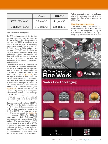
        Table 2: Comparison of package CTE.                                   e l e c t r i c a l   s i m u l a t i o n .  A  h i g h -
                                                                              frequency structure simulator (HFSS)
        the W/B package, and 48.14ºC for the
        HIFOM  package,  respectively.  The
        thermal resistance junction to ambient
        (θ JA )  of  the  HIFOM  package  was
        23.1ºC/W, and the thermal resistance
        junction  to  board  (θ JB ) was 8.4ºC/
        W. Looking at the W/B package, the
        θ JA   was  25.1ºC/W,  and  the  θ JB  was
        9.0ºC/W. Simply speaking, the HIFOM
        package had a 6~7% improved thermal
        dissipation  ability  compared  with  a
        normal  W/B  package;  this  result  is
        presumed  to  be  due  to  the  thinner
        package height.
          Package warpage was also measured
        by the shadow moiré interferometry.
        For the W/B package, the warpage was
        over 40µm with the “crying shape” at    We Take Care of the
        30ºC and at -20µm; the smile shape
        was at 260ºC (see  Figure 7a). Its      Fine Work
        warpage difference at both room and
        reflow  temperatures  was  very  high.
        However,  the  HIFOM  package  had
        no  remarkable  changes  at  room  and   Wafer Level Packaging
        reflow temperatures and its warpage
        difference  was  around  20µm    (see
        Figure 7b). These results can be
        explained by noting that no organic
        substrate resulted in a lower warpage
        in the HIFOM packages.
          T h e  c o e f f i c i e n t  o f  t h e r m a l
        expansion (CTE) of a package was
        also measured and compared using a
                                                                                  COMPONENT ASSEMBLY
        thermomechanical  analyzer  (TMA).       REDISTRIBUTION LAYER  COPPER PILLAR  COMPONENT ASSEMBLY  WAFER METALLIZATION
        A  Q400  from  TA  Instruments  was
        u sed  for  t he  T M A  mea su reme nt
        a n d  i t s  t e m p e r a t u r e  r a ng e  wa s
        20ºC  to  260ºC;  its  ramp  rate  was
        10 º C/m i n.  As  noted  i n  Table 2,
        t h e  p a c k a g e  C T E  o f  a  H I F O M
        p a ck a ge   i s   2 . 5 ~ 3 .8 p p m / º C
        less than that of a conventional W/B     ELECTROLESS PLATING  SOLDER BUMPING  WAFER THINNING  WAFER DICING
        package. With measured package CTE
        and warpage, thermal cycling (T/C)
        stresses at the BGA ball area were also
        evaluated by finite element analysis.
        As a result, the T/C stress in the
        HIFOM package was 28% lower than
        for the conventional W/B package.               pactech.com


                                                                                                             15
                                                          Chip Scale Review   January  •  February  •  2023   [ChipScaleReview.com]  15

