Page 14 - Chip Scale Review_January February_2023-digital
P. 14
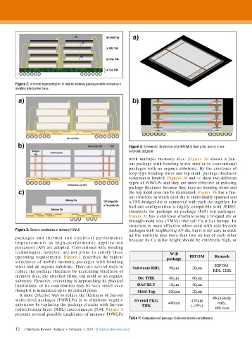
Figure 2: A simple representation of mobile memory packages with normal wire
        bonding interconnections.


                                                             Figure 4: Schematic illustration of a HIFOM a) floor plan, and b) cross-
                                                             sectional diagram.
                                                             with  multiple  memory  dies.  Figure 3a shows a fan-
                                                             out package with bonding wires similar to conventional
                                                             packages with no organic substrate. By the existence of
                                                             loop-type bonding wires and top mold, package thickness
                                                             reduction is limited. Figures 3b and 3c show two different
                                                             types of FOWLPs and they are more effective at reducing
                                                             package thickness because they have no bonding wires and
                                                             the top mold area can be minimized. Figure 3b has a fan-
                                                             out structure in which each die is individually spanned and
                                                             a TSV-bridged die is connected with each die together. Its
                                                             ball-out configuration is highly compatible with JEDEC
                                                             standards for package on package (PoP) top packages.
                                                             Figure 3c has a staircase structure using a bridged die or
                                                             through-mold vias (TMVs) like tall Cu pillar bumps. Its
                                                             structure is more effective when used with side-by-side
        Figure 3: Several candidates of memory FOWLP.        packages with neighboring AP die, but it is not easy to stack
                                                             up the multiple dies more than two on top of each other
        packages  and  ther mal  and  elect r ical  per for mance   because its Cu pillar height should be extremely high, or
        i m p r ove m e n t s   a s   h ig h - p e r for m a n c e   a p pl i c at ion
        processors (AP) are adopted. Conventional wire bonding
        technologies, however, are not prone to satisfy these
        upcoming requirements. Figure 2 describes the typical
        structures  of  mobile  memory  packages  with  bonding
        wires and an organic substrate. There are several ways to
        reduce the package thickness by decreasing thickness of
        memory dies, die attached films, top mold or an organic
        substrate. However, everything is approaching its physical
        limitations, or its contribution may be very small even
        though it is minimized up to its critical point.
          A more effective way to reduce the thickness of fan-out
        wafer-level packages (FOWLPs) is to eliminate organic
        substrates by replacing the package circuits with fan-out
        redistribution layer (RDL) interconnects [3,4]. Figure 3
        presents several possible candidates of memory FOWLPs
                                                             Table 1: Comparison of package thickness and its constituents.

        12   Chip Scale Review   January  •  February  •  2023   [ChipScaleReview.com]
        12

