Page 15 - Chip Scale Review_January February_2023-digital
P. 15
coplanarity  issues  may  occur  when   fan-out RDL to connect to two TSV-  bump  joints  and  overmold  of  each
        separated TSV-bridged dies are used   bridge dies. Six HIFOM slices on top   HIFOM slice is a little larger than the
        to  stack  three  or  more  dies.  Among   have a single RDL layer and the base   die  attached  film  of  a  conventional
        three possible candidates, the structure   HIFOM on the bottom has three RDL   package. It is expected that the BLT
        in  Figure 3b – called HIFOM, as   layers along with ball grid array (BGA)   can also be reduced by shrinking the
        noted  previously  –  was  chosen  and   balls for external interconnections.   bump  size  and  overmold  thickness
        its package character istics were   Each slice of the HIFOM is connected   later. Table 1 presents the comparison
        investigated in this study [5].    through TSV-bridged dies, which    of package thicknesses. Given that the
                                           have no real circuitry like transistors   die  thickness  is  60µm  and  the  BLT
        HIFOM structure and process        or  dynamic  random  access  memory   of the HIFOM is 40µm, the package
        flow                               (DRAM) cells, and only has a back   thickness can be significantly reduced
          F i g u r e 4  sho w s t h e d e t a i l e d   end  of  line  (BEOL)  metallization   in HIFOM.
        schematic  diagram  of  the  HIFOM   and TSV for physical interconnects.   The overall process flow of HIFOM
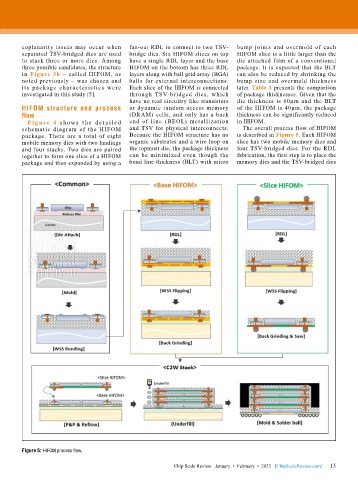
        package. There are a total of eight   Because the HIFOM structure has no   is described in Figure 5. Each HIFOM
        mobile memory dies with two landings   organic substrates and a wire loop on   slice has two mobile memory dies and
        and four stacks. Two dies are paired   the topmost die, the package thickness   four TSV-bridged dies. For the RDL
        together to form one slice of a HIFOM   can  be  minimized  even  though  the   fabrication, the first step is to place the
        package and then expanded by using a   bond line thickness (BLT) with micro   memory dies and the TSV-bridged dies


        Figure 5: HIFOM process flow.

                                                                                                             13
                                                          Chip Scale Review   January  •  February  •  2023   [ChipScaleReview.com]  13

