Page 12 - Chip Scale Review_January February_2023-digital
P. 12
Fan-out wafer-level package for memory applications


        By Ho-Young Son, Ki-Jun Sung, Jong-Hoon Kim, Kangwook Lee  [SK hynix Inc.]

        R         ecently, through-silicon   chip stackable fan-out wafer-level   Introduction


                  via (TSV) technologies
                                                                                TSV technology is very effective
                                           one of the thinnest packages that
                  have been widely used in   package  –  will  be  int roduced  as   as  a  way  to  increase  the  memor y
        high-bandwidth memory (HBM) for    ha s  bet ter  t her mal,  mecha n ical,   capacity by accommodating multiple
        high-performance computing (HPC) or   and  electrical  perfor mances  than   chips in a package—it has also been
        graphics applications and high-density   c onve nt ion a l w i r e - b on d e d t y p e   a leading advanced technology in
        memory  modules  for  DDR4/DDR5.   memory packages. This package has   me mor y  ap pl icat ion s.  Howeve r,
        For mobile memory packaging, wire   a z-height that is 15~20% thinner   TSV technology and its stacked chip
        bonding technology is still being used   than conventional wire bonding-  packages require a lot of additional
        because  of  the  high  manufacturing   based ball grid array (BGA) packages;   back-end processes and, therefore,
        cost  of  TSVs  and  the  performance   this  was  achieved  by  eliminating   i nc r e a se d  m a nu fa c t u r i ng  c o st s.
        compatibility  of  conventional  wire   organic  substrates.  For  thermal  and   Therefore, applications using TSVs are
        bonding technologies. As the overall   mechanical  characterization,  the   limited to leading-edge products like
        m o b i l e  s y s t e m  p e r f o r m a n c e  i s   thermal  resistance  and  warpage  of   HBM for HPC or graphics applications
        improved, however, the conventional   a package were evaluated. Channel   and three-dimensional stacking (3DS)
        mobile  package  may  have  several   characteristics of memory chips were   for high-density memory modules (see
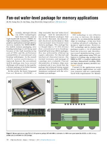
        challenges with respect to the need for   evaluated and it was found that the   Figure 1) [1,2].
        a thinner package or for better thermal   package had enhanced timing margin   Contrary to the applications noted
        and electrical performance.        and power distribution network (PDN)   above,  mobile  applications  are  still
          In this article, the Hynix Integrated   impedance compared with the wire-  cost sensitive and are consistently
        Fa n - ou t  M e m o r y  ( H I F O M )  –  a   bonded type packages.  faced with requirements for thinner


        Figure 1: Memory applications using TSVs: a) 2.5D system in package (SiP) with HBM; b) schematic of a HBM known-good stacked die (KGSD); c) a 3DS memory
        module; and d) a schematic of a 3DS package.

        10   Chip Scale Review   January  •  February  •  2023   [ChipScaleReview.com]
        10

