Page 24 - Chip Scale Review_January February_2023-digital
P. 24
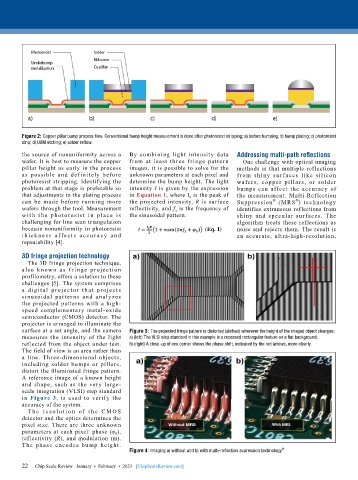
Figure 2: Copper pillar bump process flow. Conventional bump height measurement is done after photoresist stripping; a) before bumping; b) bump plating; c) photoresist
        strip; d) UBM etching; e) solder reflow.

        the source of nonuniformity across a   By  combining  light  intensity  data   Addressing multi-path reflections
        wafer. It is best to measure the copper   from  at  least  three  fringe  pattern   One challenge with optical imaging
        pillar height as early in the process   images, it is possible to solve for the   methods is that multiple reflections
        as  possible  and def initely  before   unknown parameters at each pixel and   f rom  shiny  su r faces  li ke  silicon
        photoresist stripping. Identifying the   determine the bump height. The light   wafers, copper pillars, or solder
        problem at that stage is preferable so   intensity I is given by the expression   bumps  can  affect  the  accuracy  of
        that adjustments in the plating process   in Equation 1, where I 0  is the peak of   the  measurement.  Multi-Ref lection
        can  be  made  before  running  more   the projected intensity, R is surface   Suppression  (MRS ) technology
                                                                                                  ®
                                                                                          ®
        wafers through the tool. Measurement   reflectivity, and f x  is the frequency of   identifies extraneous reflections from
        w it h t he phot ore sist i n pla ce is   the sinusoidal pattern.     shiny and specular surfaces. The
        challenging for line scan triangulation                               algorithm treats these reflections as
        because nonuniformity in photoresist                         (Eq. 1)  noise and rejects them. The result is
        t h ick n e s s a f fe c t s  a c c u r a c y a n d                   an accurate, ultra-high-resolution,
        repeatability [4].

        3D fringe projection technology
          The 3D fringe projection technique,
        also  k now n  as  f r i nge  project ion
        profilometry, offers a solution to these
        challenges [5]. The system comprises
        a  d ig it al  projector  t hat  project s
        sinusoidal patter ns and analyzes
        the  projected  patterns  with  a  high-
        speed  complementary  metal-oxide
        semiconductor (CMOS) detector. The
        projector is arranged to illuminate the
        surface at a set angle, and the camera   Figure 3: The projected fringe pattern is distorted (shifted) wherever the height of the imaged object changes;
        measures  the  intensity  of  the  light   a) (left) The VLSI step standard in this example is a recessed rectangular feature on a flat background;
        reflected from the object under test.   b) (right) A close-up of one corner shows the phase shift, indicated by the red arrows, more clearly.
        The field of view is an area rather than
        a  line.  Three-dimensional  objects,
        including  solder  bumps  or  pillars,
        distort the illuminated fringe pattern.
        A reference image of a known height
        and shape, such as the very large-
        scale integration (VLSI) step standard
        in  Figure 3, is used to verify the
        accuracy of the system.
          T h e  r e s o l u t i o n  of t h e  C M OS
        detector and the optics determines the
        pixel size. There are three unknown
        parameters at each pixel: phase (φ 0 ),
        reflectivity (R), and modulation (m).
        The  phase  encodes  bump  height.
                                                                                             ®
                                           Figure 4: Imaging a) without and b) with multi-reflection supression technology .
        22   Chip Scale Review   January  •  February  •  2023   [ChipScaleReview.com]
        22

