Page 25 - Chip Scale Review_January February_2023-digital
P. 25
an area i nstead of a li ne, it can
                                                                              simultaneously  measure  photoresist
                                                                              thickness  and  bump  height.  There
                                                                              are  geometrical  limitations  on  the
                                                                              photoresist  and  the  bump  to  enable
                                                                              accurate  bump  height  calculation.
                                                                              Currently,  the  photoresist  must  be
                                                                              at  least  45µm-thick  to  distinguish
                                                                              between  direct  ref lection  from  the
                                                                              photoresist surface and ref lection
                                                                              from the substrate. The bump height
                                                                              must  be  less  than  the  photoresist
                                                                              thickness but not too far below it.
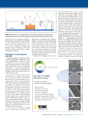
                                                                              The maximum difference between the
        Figure 5: Measurement of bump height before photoresist stripping, using light refracted through the   bump and photoresist thickness – the
        photoresist to determine the photoresist thickness and calculate bump height above the wafer surface.  depth below photoresist, as shown in
                                                                              Figure 5 – is approximately twice the
        image free from distracting artifacts.   measured to determine the substrate   width of the pillar. If the aspect ratio
        Beyond the visual appeal (see Figure   height. A portion of the incoming light   between the depth and the width is
        4),  the  MRS  system  enables  more   reflects directly off the top surface   too high, the light will deflect off the
        precise  heig ht  measu rement s.  It   of the photoresist. The rest of the   sides of the photoresist rather than
        is  currently  capable  of  measuring   light passes through the photoresist   reflect directly to the CMOS detector.
        bumps  25µm  in  diameter  with  3µm   to the wafer surface and is refracted   Bu m p  h e i g h t   u n i f o r m i t y
        lateral resolution and 0.05µm vertical   as it exits the photoresist. Given the   m e a s u r e m e n t s  f r o m  3D  f r i n g e
        (Z height) resolution.             photoresist index of refraction and data   p r o j e c t i o n  a r e  c o n s i s t e n t  w i t h
                                           from the sensor, the system measures   d a t a  f r om  a  r efe r e n c e  c o n fo c a l
        Advantages of fringe projection    the photoresist thickness.         measurement  system.  The  reference
        with MRS                             Because the imaging system scans   system  is  highly  accurate  but  takes
          Fringe projection technology offers
        greater throughput compared to line
        scan triangulation, in part because
        it  i mages  an  enti re  area  at  once
        rather than line by line. The field of
        view  and  frame  rate  are  important
        parameters.  A  system  with  multiple
        cameras and projectors operating in
        parallel at high frame rates allows the
        technology to scale.
          O u r   n e w  f r i n g e   p r o j e c t i o n
                                                       ®
        technology is rapid—collecting a      Elevate  Ni 5950
        2D scan of the wafer and height       Boric Acid Free Nickel
        measurements  of  3D  features  in  a
        single  pass.  The  system  inspects   Exceptionally stable,
        100% of the bumps on a 300mm wafer    versatile, sulfamate plating
        in minutes. By analyzing 75 million
        points every second, it achieves a
        throughput of greater than 25 wafers   •  Boric acid free
        p e r  hou r.  T he  f r i nge  proje ct ion   •  All liquid components
        system images copper pillars before   •  Very stable electrolyte
        the photoresist is stripped, either   •  Superior coplanarity
        directly  after  copper  electroplating   •  Low-stress semi-bright deposit
        or after applying a solder cap but    •  Optimum deposit up to 10 ASD
        before reflowing the solder. This is a   •  Versatile - can be used in all types of
        critical advantage because it provides      applications requiring nickel
        diagnostic data on the copper plating
        and solder bumping processes. This
        allows for process correction if the
        plating is out of tolerance.
          As the wafer is scanned at high
        s p e e d , phot o r e si s t t h ick n e s s i s   www.technic.com


                                                                                                  2/23/2022   3:16:50 PM
                                              Chip Scale Review - Elevate Ni 5959v2.indd   1
                                              Chip Scale Review - Elevate Ni 5959v2.indd   1      2/23/2022   3:16:50 PM
                                                                                                             23
                                                          Chip Scale Review   January  •  February  •  2023   [ChipScaleReview.com]  23

