Page 27 - Chip Scale Review_January February_2023-digital
P. 27
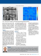
Figure 7: a) (left) A 2D image of fan-out patterns on a wafer; and b) (right) a merged image showing superimposed bump height data.
        projection  system  can  inspect  600   The technology is scalable to meet   Semiconductor Engineering, Oct.
        units  per  hour  compared  to  around   future industry roadmaps (see Figure   25, 2021. https://semiengineering.
        200  units  per  hour  for  competing   1). The second-generation MRS system   com/scaling-bump-pitches-in-
        approaches. In addition to throughput   features  more  precise  sensors  that   advanced-packaging/.
        a d v a nt a ge s ,   f r i n ge   p r o j e c t i o n   cut the resolution in  half, allowing   4. Y-S Ku, et al., “Metrology for
        technology measures both photoresist   for accurate measurement of smaller   measuring bumps in a protection
        thickness and bump height uniformity   features. As a result, fabs can commit   layer based on phase shifting fringe
        during the bumping process.        to a 100% bump height inspection on    projection,” Applied Sciences 12,
                                           every  wafer,  improving  yields  and   898, 2022. https://doi.org/10.3390/
        Summary                            reducing cost.                         app12020898.
          3D fringe projection is a nondestructive                              5. S. Feng, et al., “Calibration of
        measurement technique that combines   References                          fringe projection profilometry: a
        speed and accuracy. It can measure the   1.  S.  Enoch,  A.  Goia,  P.  Lecoq,   comparative review,” Optics and
        height of solder bumps and copper pillars   A . R ive t t i , (20 21); “ D e sig n   Lasers in Engineering 143, 106622,
        before photoresist stripping for WLP and   c on s i d e r at i on s  f or  a  n ew   2021.  htt ps://doi.org/10.1016/
        other applications. Wafers that do not   g e n e r a t i o n o f S i P M s w i t h   j.optlaseng.2021.106622
        pass uniformity screening may be able to   unprecedented timing resolution,”
        be reworked before further processing.   w w w . r e se a r c h ga t e . n et /
        Patterns  in  bump  height  uniformity   publication/348379838
        across the wafer provide valuable clues   2. K .  He y m a n ,  “ Bu m p  c o -
        to the source of the defects, identifying   planarity and inconsistencies
        whether to adjust process parameters   cause  yield,  reliability  issues,”
        or address mask or reticle errors. This   Semiconductor Engineering, Oct.
        allows  engineers  to  make  real-time   11, 2022; https://semiengineering.
        adjustments  that  reduce  waste  and   com / bu mp - co -planar it y-and-
        maximize yield. Doing so avoids the cost   inconsistencies-causing-yield-
        of scrapping large numbers of wafers that   reliability-issues/.
        might otherwise proceed through a faulty   3. M.  Lapedus,  “Scaling  bump
        plating process.                       pitches in advanced packaging,”


                       Biography
                         Tim Skunes is the VP of R&D at Nordson Test & Inspection for the CyberOptics portfolio in Minneapolis,
                       MN. Prior to this role, Tim was the Director of Product Development at CyberOptics from 2003-2010 and a
                       VP of Systems Development at Avanti Optics Corporation from 1999-2003. He holds a Masters of Electrical
                       Engineering from the U. of Minnesota. He has 26 US patents for optical measurement systems, optical
                       manufacturing, and fiber optic devices. Email tskunes@cyberoptics.com


                                                                                                             25
                                                          Chip Scale Review   January  •  February  •  2023   [ChipScaleReview.com]  25

