Page 46 - Chip Scale Review_November December_2022-digital
P. 46

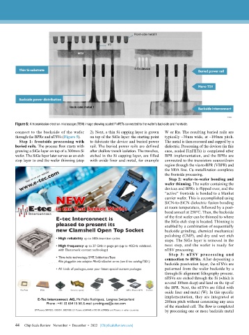
Figure 6: A transmission electron microscope (TEM) image showing scaled FinFETs connected to the wafer’s backside and frontside.
        connect to the backside of the wafer   2). Next, a thin Si capping layer is grown   W or Ru. The resulting buried rails are
        through the BPRs and nTSVs (Figure 5).  on top of the SiGe layer: the starting point   typically ~30nm wide, at ~100nm pitch.
          Step 1: frontside processing with   to fabricate the device and buried power   The metal is then recessed and capped by a
        buried rails. The process flow starts with   rail. The buried power rails are defined   dielectric. Processing of the devices (in this
        growing a SiGe layer on top of a 300mm Si   after shallow trench isolation. The trenches,   case, scaled FinFETs) is completed after
        wafer. The SiGe layer later serves as an etch   etched in the Si capping layer, are filled   BPR implementation, and the BPRs are
        stop layer to end the wafer thinning (step   with oxide liner and metal, for example   connected to the transistors source/drain
                                                                              region through the via-to-BPR (VBPR) and
                                                                              the M0A line. Cu metallization completes
                                                                              the frontside processing.
                                                                                Step 2: wafer-to-wafer bonding and
                                                                              wafer thinning. The wafer containing the
                                                                              devices and BPRs is flipped over, and the
                                                                              “active” frontside is bonded to a blanket
                                                                              carrier wafer. This is accomplished using
                                                                              SiCN-to-SiCN dielectric fusion bonding
                                                                              at room temperature, followed by a post-
                                                                              bond anneal at 250°C. Then, the backside
                                                                              of the first wafer can be thinned to where
                                                                              the SiGe etch stop is located. Thinning is
                                                                              enabled by a combination of sequentially
                                                                              backside grinding, chemical mechanical
                                                                              polishing (CMP), and dry and wet etch
                                                                              steps. The SiGe layer is removed in the
                                                                              next step, and the wafer is ready for
                                                                              nTSV processing.
                                                                                Step 3: nTSV processi ng and
                                                                              connection to BPRs. After depositing a
                                                                              backside passivation layer, the nTSVs are
                                                                              patterned from the wafer backside by a
                                                                              through-Si alignment lithography process.
                                                                              nTSVs are etched through the Si (which is
                                                                              several 100nm deep) and land on the tip of
                                                                              the BPR. Next, the nTSVs are filled with
                                                                              oxide liner and metal (W). In this specific
                                                                              implementation, they are integrated at
                   E-Tec Interconnect  AG, Mr. Pablo Rodriguez,  Lengnau Switzerland  200nm pitch without consuming any area
                       Phone : +41 32 654 15 50, E-mail: p.rodriguez@e-tec.com
                                                                              of the standard cell. The flow is completed
                                                                              by processing one or more backside metal


        44
        44   Chip Scale Review   November  •  December  •  2022   [ChipScaleReview.com]
   41   42   43   44   45   46   47   48   49   50   51