Page 41 - Chip Scale Review_November December_2022-digital
P. 41
structure leading to the highest possible
                                                                              yields while delivering up to a 10x
                                                                              reduction in capital cost for die attach.
                                                                              In addition, our patterning technology
                                                                              provides a cost-effective approach for
                                                                              scaling device interconnects for ultra-high
                                                                              density heterogeneous integration without
                                                                              the use of interposers or bridge chips.
                                                                                The next-generation of M-Series, or
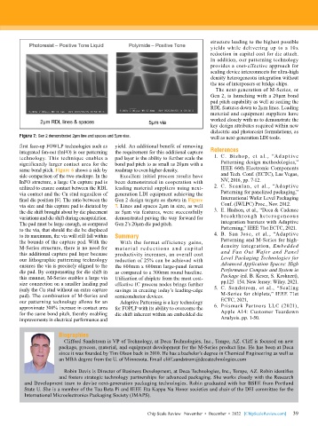
                                                                              Gen 2, is launching with a 20µm bond
                                                                              pad pitch capability as well as scaling the
                                                                              RDL features down to 2µm lines. Leading
                                                                              material and equipment suppliers have
                                                                              worked closely with us to demonstrate the
                                                                              key design attributes required within new
                                                                              dielectric and photoresist formulations, as
        Figure 7: Gen 2 demonstrated 2µm line and spaces and 5µm vias.        well as next-generation LDI tools.
        first face-up FOWLP technologies such as   yield. An additional benefit of removing
        integrated fan-out (InFO) is our patterning   the requirement for this additional capture   References
        technology. This technique enables a   pad layer is the ability to further scale the   1.  C. Bishop, et al., “Ad apt ive
        significantly larger contact area for the   bond pad pitch to as small as 20µm with a   Patterning design methodologies,”
        same bond pitch. Figure 6 shows a side by   roadmap to even higher density.  IEEE 66th Electronic Components
        side comparison of the two stackups. In the   Excellent initial process results have   and Tech. Conf. (ECTC), Las Vegas,
        InFO structure, a large Cu capture pad is   been demonstrated in cooperation with   NV, 2016, pp. 7-12.
        utilized to ensure contact between the RDL   leading material suppliers using next-  2.  C. Scanlan, et al., “Adaptive
        via contact and the Cu stud regardless of   generation LDI equipment achieving the   Patterning for panelized packaging,”
        final die position [6]. The ratio between the   Gen 2 design targets as shown in Figure   International Wafer Level Packaging
        via size and this capture pad is dictated by   7. Lines and spaces 2µm in size, as well   Conf. (IWLPC) Proc., Nov. 2012.
        the die shift brought about by die placement   as 5µm via features, were successfully   3.  E. Hudson, et al., “Deca & Cadence
        variations and die shift during encapsulation.   demonstrated paving the way forward for   brea k t h roug h heterogeneou s
        The pad must be large enough, as compared   Gen 2’s 20µm die pad pitch.   integration barriers with Adaptive
        to the via, that should the die be displaced                              Patterning,” IEEE 71st ECTC, 2021.
        to its maximum, the via will still fall within   Summary                4.  B. San Jose, et al., “Adaptive
        the bounds of the capture pad. With the   With the format efficiency gains,   Patterning and M-Series for high-
        M-Series structure, there is no need for   m at e r ia l re duct ion s a nd capit a l   density integration,  Embedded
        this additional capture pad layer because   productivity increases, an overall cost   and Fan Out Wafer and Panel
        our lithographic patterning technology   reduction of 25% can be achieved with   Level Packaging Technologies for
        ensures the via is precisely aligned to the   the 600mm x 600mm large-panel format   Advanced Application Spaces: High
        die pad. By compensating for die shift in   as compared to a 300mm round baseline.   Performance Compute and System in
        this manner, M-Series enables a large via   Utilization of chiplets from the most cost-  Package (ed. B. Keser, S. Krohnert),
        size connection on a smaller landing pad   effective IC process nodes brings further   pp.125–154. New Jersey: Wiley. 2021.
        (only the Cu stud without an extra capture   savings in creating today’s leading-edge   5.  C. Sandstrom, et al., “Scaling
        pad). The combination of M-Series and   semiconductor devices.            M-Series for chiplets,” IEEE 71st
        our patterning technology allows for an   Adaptive Patterning is a key technology   ECTC, 2021,
        approximate 300% increase in contact area   for FOPLP with its ability to overcome the   6.  Prismark Partners LLC (2021),
        for the same bond pitch, thereby enabling   die shift inherent within an embedded die   Apple A14: Customer Teardown
        improvements in electrical performance and                                Analysis. pp. 1-50.

                       Biographies
                         Clifford Sandstrom is VP of Technology, at Deca Technologies, Inc., Tempe, AZ. Cliff is focused on new
                       package, process, material, and equipment development for the M-Series product line. He has been at Deca
                       since it was founded by Tim Olson back in 2010. He has a bachelor’s degree in Chemical Engineering as well as
                       an MBA degree from the U. of Minnesota. Email cliff.sandstrom@decatechnologies.com
                         Robin Davis is Director of Business Development, at Deca Technologies, Inc., Tempe, AZ. Robin identifies
                       and fosters strategic technology partnerships for advanced packaging. She works closely with the Research
          and Development team to devise next-generation packaging technologies. Robin graduated with her BSEE from Portland
          State U. She is a member of the Tau Beta Pi and IEEE Eta Kappa Nu Honor societies and chair of the DEI committee for the
          International Microelectronics Packaging Society (IMAPS).


                                                                                                             39
                                                       Chip Scale Review   November  •  December  •  2022   [ChipScaleReview.com]  39

