Page 38 - Chip Scale Review_November December_2022-digital
P. 38
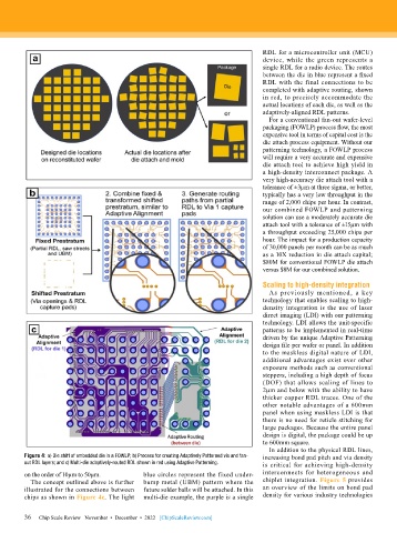
RDL for a microcontroller unit (MCU)
                                                                              device, while the green represents a
                                                                              single RDL for a radio device. The routes
                                                                              between the die in blue represent a fixed
                                                                              RDL with the final connections to be
                                                                              completed with adaptive routing, shown
                                                                              in red, to precisely accommodate the
                                                                              actual locations of each die, as well as the
                                                                              adaptively-aligned RDL patterns.
                                                                                For a conventional fan-out wafer-level
                                                                              packaging (FOWLP) process flow, the most
                                                                              expensive tool in terms of capital cost is the
                                                                              die attach process equipment. Without our
                                                                              patterning technology, a FOWLP process
                                                                              will require a very accurate and expensive
                                                                              die attach tool to achieve high yield in
                                                                              a high-density interconnect package. A
                                                                              very high-accuracy die attach tool with a
                                                                              tolerance of ±3µm at three sigma, or better,
                                                                              typically has a very low throughput in the
                                                                              range of 2,000 chips per hour. In contrast,
                                                                              our combined FOWLP and patterning
                                                                              solution can use a moderately accurate die
                                                                              attach tool with a tolerance of ±15µm with
                                                                              a throughput exceeding 25,000 chips per
                                                                              hour. The impact for a production capacity
                                                                              of 30,000 panels per month can be as much
                                                                              as a 10X reduction in die attach capital;
                                                                              $80M for conventional FOWLP die attach
                                                                              versus $8M for our combined solution.
                                                                              Scaling to high-density integration
                                                                                As previously mentioned, a key
                                                                              technology that enables scaling to high-
                                                                              density integration is the use of laser
                                                                              direct imaging (LDI) with our patterning
                                                                              technology. LDI allows the unit-specific
                                                                              patterns to be implemented in real-time
                                                                              driven by the unique Adaptive Patterning
                                                                              design file per wafer or panel. In addition
                                                                              to the maskless digital nature of LDI,
                                                                              additional advantages exist over other
                                                                              exposure methods such as conventional
                                                                              steppers, including a high depth of focus
                                                                              (DOF) that allows scaling of lines to
                                                                              2µm and below with the ability to have
                                                                              thicker copper RDL traces. One of the
                                                                              other notable advantages of a 600mm
                                                                              panel when using maskless LDI is that
                                                                              there is no need for reticle stitching for
                                                                              large packages. Because the entire panel
                                                                              design is digital, the package could be up
                                                                              to 600mm square.
                                                                                In addition to the physical RDL lines,
        Figure 4: a) Die shift of embedded die in a FOWLP; b) Process for creating Adaptively Patterned via and fan-  increasing bond pad pitch and via density
        out RDL layers; and c) Multi-die adaptively-routed RDL shown in red using Adaptive Patterning.  is critical for achieving high-density
        on the order of 10μm to 50μm.      blue circles represent the fixed under-  interconnects for heterogeneous and
          The concept outlined above is further   bump metal (UBM) pattern where the   chiplet integration. Figure 5 provides
        illustrated for the connections between   future solder balls will be attached. In this   an overview of the limits on bond pad
        chips as shown in Figure 4c. The light   multi-die example, the purple is a single   density for various industry technologies


        36
        36   Chip Scale Review   November  •  December  •  2022   [ChipScaleReview.com]

