Page 40 - Chip Scale Review_November December_2022-digital
P. 40
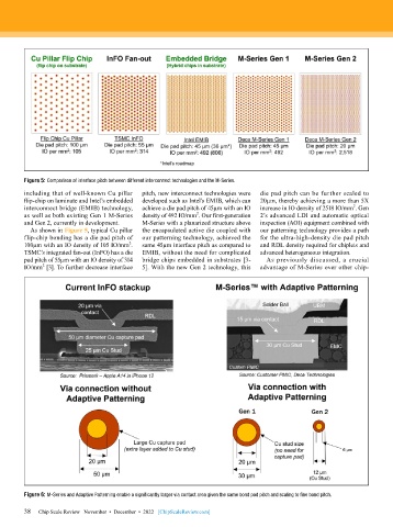
Figure 5: Comparison of interface pitch between different interconnect technologies and the M-Series.
        including that of well-known Cu pillar   pitch, new interconnect technologies were   die pad pitch can be further scaled to
        flip-chip on laminate and Intel’s embedded   developed such as Intel’s EMIB, which can   20µm, thereby achieving a more than 5X
                                                                                                          2
        interconnect bridge (EMIB) technology,   achieve a die pad pitch of 45µm with an IO   increase in IO density of 2518 IO/mm . Gen
                                                            2
        as well as both existing Gen 1 M-Series   density of 492 IO/mm . Our first-generation   2’s advanced LDI and automatic optical
        and Gen 2, currently in development.  M-Series with a planarized structure above   inspection (AOI) equipment combined with
          As shown in Figure 5, typical Cu pillar   the encapsulated active die coupled with   our patterning technology provides a path
        flip-chip bonding has a die pad pitch of   our patterning technology, achieved the   for the ultra-high-density die pad pitch
                                       2
        100µm with an IO density of 105 IO/mm .   same 45µm interface pitch as compared to   and RDL density required for chiplets and
        TSMC’s integrated fan-out (InFO) has a die   EMIB, without the need for complicated   advanced heterogeneous integration.
        pad pitch of 55µm with an IO density of 314   bridge chips embedded in substrates [3-  As previously discussed, a crucial
        IO/mm  [3]. To further decrease interface   5]. With the new Gen 2 technology, this   advantage of M-Series over other chip-
              2


        Figure 6: M-Series and Adaptive Patterning enable a significantly larger via contact area given the same bond pad pitch and scaling to fine bond pitch.

        38
        38   Chip Scale Review   November  •  December  •  2022   [ChipScaleReview.com]

