Page 44 - Chip Scale Review_November December_2022-digital
P. 44
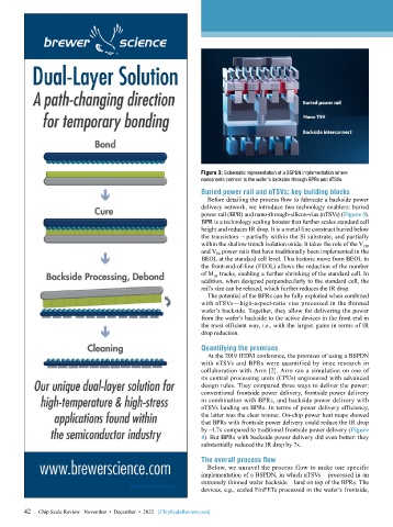
Figure 3: Schematic representation of a BSPDN implementation where
                                                             nanosheets connect to the wafer’s backside through BPRs and nTSVs.
                                                             Buried power rail and nTSVs: key building blocks
                                                               Before detailing the process flow to fabricate a backside power
                                                             delivery network, we introduce two technology enablers: buried
                                                             power rail (BPR) and nano-through-silicon-vias (nTSVs) (Figure 3).
                                                             BPR is a technology scaling booster that further scales standard cell
                                                             height and reduces IR drop. It is a metal line construct buried below
                                                             the transistors – partially within the Si substrate, and partially
                                                             within the shallow trench isolation oxide. It takes the role of the V DD
                                                             and V SS  power rails that have traditionally been implemented in the
                                                             BEOL at the standard cell level. This historic move from BEOL to
                                                             the front-end-of-line (FEOL) allows the reduction of the number
                                                             of M int  tracks, enabling a further shrinking of the standard cell. In
                                                             addition, when designed perpendicularly to the standard cell, the
                                                             rail’s size can be relaxed, which further reduces the IR drop.
                                                               The potential of the BPRs can be fully exploited when combined
                                                             with nTSVs—high-aspect-ratio vias processed in the thinned
                                                             wafer’s backside. Together, they allow for delivering the power
                                                             from the wafer’s backside to the active devices in the front end in
                                                             the most efficient way, i.e., with the largest gains in terms of IR
                                                             drop reduction.

                                                             Quantifying the promises
                                                               At the 2019 IEDM conference, the promises of using a BSPDN
                                                             with nTSVs and BPRs were quantified by imec research in
                                                             collaboration with Arm [2]. Arm ran a simulation on one of
                                                             its central processing units (CPUs) engineered with advanced
                                                             design rules. They compared three ways to deliver the power:
                                                             conventional frontside power delivery, frontside power delivery
                                                             in combination with BPRs, and backside power delivery with
                                                             nTSVs landing on BPRs. In terms of power delivery efficiency,
                                                             the latter was the clear winner. On-chip power heat maps showed
                                                             that BPRs with frontside power delivery could reduce the IR drop
                                                             by ~1.7x compared to traditional frontside power delivery (Figure
                                                             4). But BPRs with backside power delivery did even better: they
                                                             substantially reduced the IR drop by 7x.
                                                             The overall process flow
                                                               Below, we unravel the process flow to make one specific
                                                             implementation of a BSPDN, in which nTSVs – processed in an
                                                             extremely thinned wafer backside – land on top of the BPRs. The
                                                             devices, e.g., scaled FinFETs processed in the wafer’s frontside,


        42
        42   Chip Scale Review   November  •  December  •  2022   [ChipScaleReview.com]

