Page 43 - Chip Scale Review_November December_2022-digital
P. 43
Powering chips from the backside


        By Naoto Horiguchi, Eric Beyne  [imec]

        A         power delivery network is


                  designed to provide power
                  su p p l y  a n d  r e f e r e n c e
        voltage (i.e., V DD  and V SS ) to the active
        devices  on  the  die  most  efficiently.
        Traditionally, it is realized as a
        network of low-resistive metal wires
        fabricated through back-end-of-line
        (BEOL) processing on the frontside of
        the wafer. The power delivery network
        shares this space with the signal
        network, i.e., the interconnects that
        are designed to transport the signal.
          To deliver power from the package
        to the transistors, electrons traverse
        all  15-20  layers  of  the  BEOL  stack
        through metal wires and vias that get
        increasingly narrow (hence, more
        resist ive) when approach i ng t he
        transistors.  On  their  way, they lose
        energy, resulting in a power delivery,
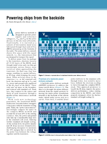
        or IR drop, when bringing the power   Figure 1: Schematic representation of a traditional frontside power delivery network.
        down.  When  arriving  closer  to  the
        transistor, i.e., at the standard cell   Promises of a backside power   power delivery to the standard cells
        level, the electrons end up in V DD  and   delivery network           through wider, less resistive metal
        V SS  power and ground rails organized   A backside power delivery network   lines, without the electrons needing
        in the M int  layer of the BEOL. These   (BSPDN) promises to address the   to travel through the complex BEOL
        rails take up space at the boundary   issues noted above (Figure 2). The   stack. This approach promises to
        and between each standard cell. From   idea is to decouple the power delivery   benefit the IR drop, improve the power
        here, they connect to the source and   network from the signal network by   delivery performance, reduce routing
        drain of each transistor through  a   moving the entire power distribution   congestion in the BEOL, and when
        middle-of-line interconnect network   network to the backside of the silicon   properly designed, allow for further
        (Figure 1).                        wafer, which today serves only as a   standard cell height scaling [1].
          W i t h e a c h n e w t e c h n o l o g y   carrier. From there, it enables direct
        generation, the traditional BEOL
        architecture described above struggles
        to keep pace with the transistor scaling
        path. Today, the “power interconnects”
        increasingly compete for space in
        t he complex BEOL net work a nd
        account for at least 20% of the routing
        resources. Also, the power and ground
        rails take up a considerably large area
        at the standard cell level, limiting
        further standard cell height scaling.
        At the system level, the power density
        and IR drop increase dramatically,
        challenging designers to maintain
        the 10% margin that is allowed for
        the power loss between the voltage
        regulator and the transistors.
                                           Figure 2: A BSPDN allows for decoupling the power delivery from the signal network.

                                                                                                             41
                                                       Chip Scale Review   November  •  December  •  2022   [ChipScaleReview.com]  41

